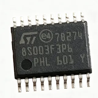
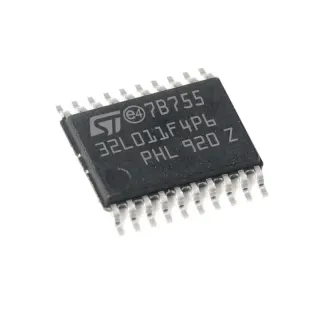
STM32G031F4P6 - 64MHz Cortex-M0+ 16KB MCU | STMicroelectronics
Артикул: STM32G031F4P6 ✓ АктивенSTM32G031F4P6 Обзор
A microcontroller is a programmable semiconductor that integrates a CPU core, nonvolatile program memory, volatile data memory, and peripherals on one device. Within the product hierarchy, the STM32G031F4P6 is an ARM Cortex-M0+ MCU, an STM32G0-series microcontroller, and a 32-bit embedded-control semiconductor. Its combination of 64 MHz processing, 16 KB Flash, and 8 KB RAM is suitable for small control systems, embedded accessories, instrumentation, and compact consumer products.
Verified distributor information identifies the part as a 3 V, 20-TSSOP device with 16 KB Flash and 8 KB RAM. The 20-pin TSSOP format supports compact PCB layouts while retaining accessible peripheral connections. The exact pin names, voltage limits, peripheral inventory, current ratings, and environmental limits were not included in the supplied source snippets and therefore require confirmation from the manufacturer datasheet before a new design is released.
The Cortex-M0+ architecture provides a 32-bit processing environment with an emphasis on efficient embedded control. A 64 MHz clock gives the processor more timing headroom for input sampling, state-machine logic, communication tasks, and control-loop updates than lower-frequency microcontrollers. Memory use is the main design constraint: 16 KB Flash must hold the bootloader, application code, and constant data, while 8 KB RAM must support stack depth, working variables, buffers, and peripheral data.
Typical uses include small motor and relay controllers, sensor-hub nodes, compact industrial modules, communication-assisted accessories, and low-cost embedded products where a full STM32G0 system is unnecessary. Designers should include external flash only if the application exceeds the internal memory budget. Software migration decisions should also account for peripheral differences between STM32G0 variants, even when several parts share the same package.
Before layout or firmware release, verify the exact pin assignment, alternate-function mapping, decoupling requirements, operating-voltage limits, exposed programming/test pins, and absolute maximum ratings in the manufacturer datasheet. The supplied records confirm the core identity, memory configuration, clock, package, and a verified LCSC unit price of $0.6593 as of 2026-10-30, but they do not provide complete electrical or pinout tables.
This page combines verified distributor specifications, sourced replacement candidates, procurement data, and practical memory-budget guidance. It also identifies where manufacturer-level verification is mandatory, preventing incomplete distributor snippets from being mistaken for complete production specifications.
Аналоги без доработки для STM32G031F4P6 — тот же корпус, pin-to-pin совместимость. Компоненты в других корпусах, требующие переработки PCB, исключены.
Варианты в этой серии
Модели той же серии, совместимые без доработки с STM32G031F4P6 (тот же форм-фактор и посадочное место) — отличается по Flash Memory, Package.
STM32G031F8P6
✅ Прямая заменаУточнить цену
Открыть даташит →STM32G041F6P6TR
✅ Прямая замена📋 Справочный аналог (нет в каталоге)
STM32G031F6P7TR
✅ Прямая замена📋 Справочный аналог (нет в каталоге)
STM32G031F4P6 Максимальные параметры и электрические характеристики
| Product Type | 32-bit ARM Cortex-M0+ microcontroller |
| Product Series | STM32G0 |
| CPU Core | ARM Cortex-M0+ |
| Maximum CPU Frequency | 64 MHz |
| Architecture | 32-bit |
| Flash Memory | 16 KB (16K x 8) |
| SRAM | 8 KB |
| Operating Voltage | 3 V |
| Корпус | 20-TSSOP |
| Package Width | 4.40 mm |
| Lead Pitch | 0.173 mm |
| Тип монтажа | Surface mount |
Руководство по цоколевке STM32G031F4P6 в корпусе 4.40 mm
Цоколевка для STM32G031F4P6 (корпус 4.40 mm). Эта цифровая ИС включает выводы GPIO, интерфейсы связи (UART, SPI, I2C) и выводы питания. Обратитесь к техническому описанию производителя для альтернативных функций выводов и вариантов конфигурации. Необходимо для проектирования встраиваемых систем и трассировки печатных плат.

Нет подробных данных о распиновке для STM32G031F4P6.
Обратитесь к даташиту для полной конфигурации выводов.
Типичное применение
STM32G031F4P6 подходит для 6 применениеs: Compact Sensor-Control Node, Small Motor and Relay Controller, Communication-Assisted Embedded Accessory, Low-Cost Consumer Control Module, Industrial Measurement Front End, Low-Power Embedded Control.
Compact Sensor-Control Node
The STM32G031F4P6 fits a small sensor-control node when the firmware can operate within its verified 16 KB Flash and 8 KB RAM limits. The 64 MHz ARM Cortex-M0+ core can manage sensor polling, digital filtering, state-machine logic, and local status indication without requiring a larger MCU. Its 20-TSSOP package also helps minimize board width in space-constrained products. The design should budget SRAM for the stack, acquisition buffers, and communication descriptors before adding functions. Because the supplied records do not confirm the exact ADC channels, GPIO count, or peripheral map, engineers must verify those resources in the manufacturer datasheet and retain a memory margin for future code growth.
Small Motor and Relay Controller
The STM32G031F4P6 is a candidate for a compact motor or relay controller because its 64 MHz Cortex-M0+ processor provides useful timing headroom for debouncing, state transitions, fault monitoring, and actuator sequencing. The 16 KB Flash footprint is appropriate for a focused controller rather than a feature-rich user interface, while 8 KB RAM can support a bounded control state machine. A 20-TSSOP package permits a relatively compact controller PCB. The key trade-off is memory: PWM resources, timer channels, protection limits, and pin assignments were not available in the supplied snippets and must be confirmed. Production firmware should also include fail-safe de-energization behavior rather than relying solely on nominal software timing.
Communication-Assisted Embedded Accessory
The STM32G031F4P6 can support a communication-assisted embedded accessory when the product requires a compact general-purpose controller rather than a high-end system-on-chip. The verified 64 MHz Cortex-M0+ core is suitable for protocol framing, command parsing, status management, and coordination of peripheral actions. Its 16 KB Flash and 8 KB RAM constrain the number of simultaneous protocol stacks and buffered data volumes, so protocol selection and buffer sizing must be planned conservatively. The 3 V 20-TSSOP construction aligns with compact low-voltage designs. Exact USART, SPI, and I2C counts were not included in the supplied source, making pin multiplexing and peripheral availability a mandatory datasheet check before interface assignment.
Low-Cost Consumer Control Module
The STM32G031F4P6 is well suited to a focused consumer-control module combining a 64 MHz Cortex-M0+ core, 16 KB Flash, and 8 KB RAM in 20-TSSOP. It can handle button logic, indicators, simple timing, and limited configuration while keeping the component count and board size modest. The verified LCSC starting price of $0.6593 as of 2026-10-30 makes cost evaluation relevant for high-volume designs, but that figure should be reconfirmed. Firmware should avoid features likely to exhaust Flash or SRAM, and the product team should verify operating-temperature limits, ADC performance, and low-power behavior from the manufacturer datasheet before committing to a consumer operating environment.
Industrial Measurement Front End
The STM32G031F4P6 may serve as the control element in a small industrial measurement front end when the signal-processing workload is modest and the unit must coexist with analog circuitry. The 64 MHz Cortex-M0+ core can execute acquisition sequencing, calibration logic, digital filtering, and communication tasks, while the 20-TSSOP package keeps the digital section compact. However, the verified 16 KB Flash and 8 KB RAM require disciplined allocation across code, buffers, and calibration tables. ADC resolution, input count, reference accuracy, analog noise, and operating-temperature limits were not supplied and are essential for measurement integrity. Do not infer measurement performance from the MCU clock frequency; validate the complete analog signal chain and noise behavior on hardware.
Low-Power Embedded Control
The STM32G031F4P6 is a potential fit for low-power embedded control because the STM32G0 family targets resource-efficient applications and the device operates from a stated 3 V supply. The 64 MHz core provides performance headroom without requiring a larger memory footprint, while 16 KB Flash and 8 KB RAM constrain the design toward focused control loops. The supplied source does not disclose sleep-mode current, wake-up sources, or operating-mode power figures, so battery-life calculations cannot be completed from the available evidence. Confirm those values and the exact GPIO retention behavior in the manufacturer datasheet, and use the MCU's low-power modes only after measuring the complete board rather than the bare component.
Справочные инженерные данные для STM32G031F4P6 — сравнение, рекомендации по проектированию и информация о соответствии.
Руководство по выбору
Сравнение с аналогами
| Параметр | Этот товар | STM32G031F8P6 | STM32G041F6P6TR | STM32G031F6P7TR |
|---|---|---|---|---|
| Package | 20-TSSOP | 20-TSSOP | 20-TSSOP | 20-TSSOP |
| Brand | STMicroelectronics | STMicroelectronics | STMicroelectronics | STMicroelectronics |
| CPU Core | ARM Cortex-M0+ | ARM Cortex-M0+ | ARM Cortex-M0+ | ARM Cortex-M0+ |
| Product Series | STM32G0 | STM32G0 | STM32G0 | STM32G0 |
Ключевые отличия
- Exact 16 KB Flash allocation for focused embedded firmware (против STM32G031F8P6)
- Confirmed 8 KB SRAM configuration (против STM32G041F6P6TR)
- Documented 64 MHz Cortex-M0+ performance target (против STM32G031F6P7TR)
Заметки по проектированию
Budget the 16 KB Flash and 8 KB SRAM before committing to the firmware architecture. Reserve SRAM for the stack, interrupt context, communication buffers, and worst-case control state rather than estimating only steady-state variables. Track linker-map growth during development and keep sufficient margin for bootloader integration and field updates. The verified 3 V operating point also requires a supply source capable of meeting the MCU's input-voltage and transient limits, which must be confirmed from the manufacturer datasheet.
Use the official 20-TSSOP land pattern and verify its dimensions against the manufacturer package drawing; the supplied distributor snippets confirm 4.40 mm package width and 0.173 mm lead pitch but do not provide the complete footprint. Place required decoupling capacitors close to the corresponding supply pins and maintain short return paths for high-frequency current. Check programming and debug access before routing the PCB, and confirm whether any pins have restricted analog, debug, or boot functions in the manufacturer pinout.
Do not treat a shared TSSOP package as proof that any STM32G0 candidate is automatically drop-in compatible. The alternative candidates may differ in Flash capacity, peripheral inventory, interrupt implementation, or ordering suffix. Compare the numbered pinout, alternate functions, supply limits, clock tree, boot behavior, and peripheral addresses, then compile and test the firmware on each proposed device. Also do not infer automotive qualification, RoHS compliance, or temperature grade from the base MPN without current manufacturer documentation.
Информация о соответствии
The supplied distributor snippets do not contain verifiable compliance declarations or automotive qualification evidence. Obtain current material-compliance and qualification documents from STMicroelectronics before production release.