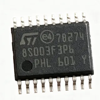
STM8S103F3P6 - 8-bit 16MHz MCU, 8KB Flash, 20-TSSOP | STMicroelectronics
Артикул: STM8S103F3P6 ✓ Активен| Кол-во | Цена за ед. | Итого |
|---|---|---|
| 1 | $1.85 | $1,85 |
| 10 | $1.62 | $16,20 |
| 100 | $1.28 | $128,00 |
| 500 | $1.05 | $525,00 |
| 1.000 | $0.92 | $920,00 |
STM8S103F3P6 Обзор
An 8-bit microcontroller (MCU) is a single-chip computer that integrates a CPU, memory, and peripheral interfaces. The STM8 core uses an advanced Harvard architecture with a 16-bit instruction word and 32-bit program counter extension for efficient code density. The "Access line" designation indicates this part targets cost-optimized designs with sufficient peripherals for general control tasks. This positions the STM8S103F3P6 within the broader taxonomy: MCU -> 8-bit microcontroller -> STM8 family -> STM8S access line -> STMicroelectronics 8-bit portfolio.
Key features include 8 KB Flash with in-application programming (I2AP) capability, 640-byte true data EEPROM rated for 300 k write/erase cycles, a 10-bit ADC with up to 5 channels, and a 4-channel 16-bit PWM/timer structure supporting capture, compare, and one-pulse modes. The integrated SWIM debug interface and on-chip watchdog with window option simplify development and field reliability. The 20-pin TSSOP package offers a compact 6.5 mm × 4.4 mm footprint suitable for space-constrained PCBs.
Typical applications include low-cost consumer appliances, sensor interface nodes, LED lighting controllers, battery chargers, simple motor drivers, and replacement of legacy 8051 or PIC16 designs. The wide 2.95-5.5 V supply range also supports 3.3 V and 5 V industrial systems without level shifters.
Designers should note that the STM8S103F3P6 (industrial grade, -40 °C to 85 °C) and the STM8S003F3P6 differ in feature set; the '103 part includes a beeper and AWU peripherals absent on the '003. For higher memory needs, the STM8S105 series provides 32 KB Flash in larger packages. This page synthesizes distributor pricing, drop-in alternatives, and design notes not found in the manufacturer datasheet alone.
Аналоги без доработки для STM8S103F3P6 — тот же корпус, pin-to-pin совместимость. Компоненты в других корпусах, требующие переработки PCB, исключены.
Варианты в этой серии
Модели той же серии, совместимые без доработки с STM8S103F3P6 (тот же форм-фактор и посадочное место) — отличается по Core, Operating Temperature, Package, ADC Resolution, Communication Interfaces.
Инструмент быстрого сравнения — выберите альтернативные компоненты для сравнения бок о бок:
STM8S103F2P6
✅ Прямая замена📋 Справочный аналог (нет в каталоге)
STM8S003F3P6
✅ Прямая замена✓ В наличии
$0.36 / шт.
Открыть даташит →STM8S103F3P6TR
✅ Прямая замена📋 Справочный аналог (нет в каталоге)
STM8S103F3P6 Максимальные параметры и электрические характеристики
| Core | STM8 8-bit (Harvard architecture) |
| Максимальная тактовая частота | 16 MHz |
| Program Memory (Flash) | 8 KB |
| Data EEPROM | 640 B |
| RAM | 1 KB |
| Data EEPROM Endurance | 300 k cycles |
| Supply Voltage Range | 2.95 V to 5.5 V |
| Рабочая температура | -40 °C to +85 °C |
| Number of I/O Pins | 16 |
| ADC | 10-bit, up to 5 channels |
| Timers | 3 × 16-bit (TIM1, TIM2, TIM4) |
| Communication Interfaces | UART, SPI, I²C |
| Корпус | 20-TSSOP |
| Debug Interface | SWIM (single-wire) |
| Watchdog | Window watchdog + independent WDG |
| Тип монтажа | Surface Mount |
Конфигурация выводов STM8S103F3P6
| Контакт 1 | VDD — Supply voltage (2.95 V to 5.5 V) |
| Контакт 2 | PA1 — Port A bit 1 / SWIM data |
| Контакт 3 | PA2 — Port A bit 2 / oscillator output |
| Контакт 4 | PD1 — Port D bit 1 |
| Контакт 5 | PB0 — Port B bit 0 / AIN0 / TIM1_CH1N |
| Контакт 6 | PB1 — Port B bit 1 / AIN1 |
| Контакт 7 | PB2 — Port B bit 2 / AIN2 |
| Контакт 8 | PB3 — Port B bit 3 / AIN3 |
| Контакт 9 | PB4 — Port B bit 4 / AIN4 |
| Контакт 10 | PB5 — Port B bit 5 / BEEPER output |
| Контакт 11 | PB6 — Port B bit 6 / I²C SDA |
| Контакт 12 | PB7 — Port B bit 7 / I²C SCL |
| Контакт 13 | PC1 — Port C bit 1 / TIM1_CH1 |
| Контакт 14 | PC2 — Port C bit 2 / TIM1_CH2 |
| Контакт 15 | PC3 — Port C bit 3 / TIM1_CH3 |
| Контакт 16 | PC4 — Port C bit 4 / TIM1_CH4 |
| Контакт 17 | PC5 — Port C bit 5 / SPI SCK |
| Контакт 18 | PC6 — Port C bit 6 / SPI MOSI |
| Контакт 19 | PC7 — Port C bit 7 / SPI MISO |
| Контакт 20 | VSS — Ground |
Типичное применение
STM8S103F3P6 подходит для 6 применениеs: Consumer Appliance Control, LED Lighting Driver, Battery Charger Controller, Sensor Interface Module, Replacement for Legacy 8051 / PIC16 Designs, Simple Motor Driver / BLDC Companion.
Consumer Appliance Control
The STM8S103F3P6 fits cost-sensitive white-goods and small-appliance controllers thanks to its 8 KB Flash, 16 MHz core, and integrated peripherals that replace discrete glue logic. With 16 GPIO pins, a beeper driver, and a 10-bit ADC for sensing temperature or voltage, the part handles keypad scanning, triac zero-cross control, and indicator PWM in a single chip. Typical subsystems: washing-machine user interface, microwave keypad, fan speed controller, and rice-cooker thermostat.
Рекомендуется
LED Lighting Driver
The STM8S103F3P6 drives multichannel LED lighting by combining its 4-channel 16-bit PWM timer with 10-bit ADC feedback for closed-loop current regulation. The 5.5 V tolerance supports 5 V analog reference designs for photometric sensors, while the 16 MHz core is fast enough to run DMX-style or PWM-dim protocols. Integrated beeper can signal fault conditions without an extra timer.
Рекомендуется
Battery Charger Controller
For NiMH, Li-ion, or lead-acid charger designs, the STM8S103F3P6 offers the ADC for V/I sensing, a PWM channel for synchronous buck or linear regulation, and the AWU peripheral for sleep-mode monitoring. The 640-byte true EEPROM stores charging profiles and cycle counters without external memory. UART output can report state to a host MCU or BLE module.
Рекомендуется
Sensor Interface Module
Industrial sensor nodes leverage the STM8S103F3P6 I²C/SPI master capability plus the 10-bit ADC to read multiple analog and digital sensors. UART enables Modbus RTU slave communication on RS-485 segments, and the 8 KB Flash holds calibration tables for thermocouple or bridge-sensor linearization. The -40 °C to +85 °C industrial range supports outdoor and factory-floor deployment.
Рекомендуется
Replacement for Legacy 8051 / PIC16 Designs
Designers moving legacy 8051 or PIC16 firmware gain a modern toolchain and on-chip peripherals when migrating to the STM8S103F3P6. With 8 KB Flash, 1 KB RAM, three timers, and a SWIM debug interface, it covers most small-control applications while offering better interrupt latency and a true C compiler. The 20-TSSOP package drop-in fits existing 8051 footprints when the OEM PCB was designed for an SOP-20 MCU.
Рекомендуется
Simple Motor Driver / BLDC Companion
The STM8S103F3P6 acts as a user-interface and safety companion to a dedicated motor-driver IC in low-power BLDC, stepper, or brushed-DC applications. It runs PWM command generation, button/encoder input, fault monitoring via ADC, and UART comms to a host controller. The beeper provides audible stall alarms without external timer hardware.
Рекомендуется
Сводка рекомендуемых товаров
Справочные инженерные данные для STM8S103F3P6 — сравнение, рекомендации по проектированию и информация о соответствии.
Руководство по выбору
Сравнение с аналогами
| Параметр | Этот товар | STM8S103F2P6 | STM8S003F3P6 | STM8S103F3P6TR |
|---|---|---|---|---|
| Brand | STMicroelectronics | STMicroelectronics | STMicroelectronics | STMicroelectronics |
| Package | 20-TSSOP | 20-TSSOP - same | 20-TSSOP - same | 20-TSSOP - same |
| Flash Memory | 8 KB | 4 KB | 8 KB | 8 KB |
| RAM | 1 KB | 1 KB | 1 KB | 1 KB |
| EEPROM | 640 B | 640 B | 640 B | 640 B |
| Core Clock | 16 MHz | 16 MHz | 16 MHz | 16 MHz |
| Beeper Peripheral | Yes | Yes | No | Yes |
| Operating Temperature | -40 °C to +85 °C | -40 °C to +85 °C | -40 °C to +85 °C | -40 °C to +85 °C |
Ключевые отличия
- True data EEPROM on-chip (против STM8S003F3P6)
- Higher Flash density vs F2 sibling (против STM8S103F2P6)
- Industrial temperature grade as standard (против STM8S103F3P3)
Заметки по проектированию
The STM8S103F3P6 has internal voltage regulation derived from VDD; decouple VDD/VSS with a 100 nF ceramic capacitor placed within 5 mm of the pins plus a bulk 4.7 µF tantalum or electrolytic for switching transients. The AWU peripheral draws only a few µA from VDD in halt mode, but peripherals left clocked can multiply supply current. Activate PWR_HSITRIM_Q1..Q4 settings and disable unused peripherals in the CLK_PCKENR register to minimize run current.
For the 20-TSSOP package, route the SWIM pin (PA1) directly to a 4-pin test header to keep programming accessible without rework. Place the external reset pull-up (10 kΩ to VDD) close to the NRST pin if the application uses external reset. The 16 MHz HSE crystal or resonator, if used, should sit adjacent to pins PA1/PA2 with short symmetric traces and a ground guard ring for EMI robustness.
Do not confuse the STM8S103F3P6 (industrial -40 °C to +85 °C, with beeper/AWU) with the STM8S003F3P6 (no beeper/AWU) or STM8S103F3P3 (commercial 0 °C to 70 °C) - same package, different peripheral set or temperature grade. When migrating firmware from STM8S105 series, verify ADC channel count (5 vs 16) and timer resources. The SWIM debug interface is single-wire; do not add external pull-ups on PA1 that exceed 10 kΩ or debug will fail.
Информация о соответствии
RoHS/REACH compliant per ST product page; AEC-Q100 not qualified (consumer/industrial grade); lead-free TSSOP package per JEDEC J-STD-020 MSL1