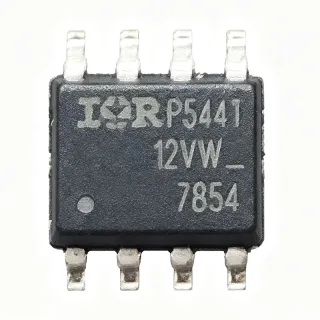
STS7DNH3LL - Dual N-Channel 30V MOSFET, 0.018Ω, 7A | STMicroelectronics
Артикул: STS7DNH3LL ✓ Активен| Кол-во | Цена за ед. | Итого |
|---|---|---|
| 1 | $0.92 | $0,92 |
| 10 | $0.78 | $7,80 |
| 100 | $0.65 | $65,00 |
| 500 | $0.52 | $260,00 |
| 1.000 | $0.41 | $410,00 |
STS7DNH3LL Обзор
A Power MOSFET is a voltage-controlled semiconductor switch that uses an electric field at the gate to control current flow between drain and source, enabling high-efficiency power conversion at switching frequencies that mechanical or bipolar devices cannot achieve. Within the broader semiconductor taxonomy, a Power MOSFET belongs to the discrete transistor family (transistor -> discrete semiconductor -> semiconductor), with the sub-class of enhancement-mode N-channel devices dominating low-voltage synchronous-rectifier designs because N-channel carriers exhibit roughly three times higher mobility than P-channel carriers, lowering conduction loss for a given silicon area.
Key features of the STS7DNH3LL include 0.018 Ω typical on-resistance at VGS = 10 V, 30 V VDS max rating, ±20 V VGS rating, low gate charge optimized for STripFET III generation, and an integrated dual-FET topology that halves board area versus two discrete DPAK devices. The SO-8 package supports a maximum power dissipation of approximately 2.5 W per channel with proper copper thermal management, and the device is rated for operation across -55°C to +175°C junction temperature for harsh-environment industrial loads.
Architecturally, the STS7DNH3LL uses STMicroelectronics' third-generation STripFET III trench-gate process, which reduces the figure-of-merit RDS(on) × Qg compared to earlier planar generations. This directly translates into lower switching and conduction losses in high-frequency buck and synchronous-rectifier applications. The integrated monolithic dual-die construction also reduces parasitic source inductance relative to discrete pairs, which improves switching performance and reduces ringing on the gate drive waveform.
Typical applications include synchronous rectification in 12 V buck converters for telecom and server point-of-load rails, low-voltage DC motor control in robotics and drones, OR-ing and hot-swap circuits on multi-rail backplanes, and high-efficiency battery management in portable electronics and e-bike motor controllers. The dual-FET topology is particularly valuable where PCB real estate is at a premium.
When designing with this device, place the gate-drive return paths directly over the source pad to minimize parasitic inductance, and ensure the gate drive voltage is sequenced properly to prevent simultaneous turn-on of both channels. The SO-8 thermal pad is the drain terminal for both FETs, so the PCB copper pour doubles as both a thermal dissipation path and a low-impedance drain connection.
Аналоги без доработки для STS7DNH3LL — тот же корпус, pin-to-pin совместимость. Компоненты в других корпусах, требующие переработки PCB, исключены.
Варианты в этой серии
Модели той же серии, совместимые без доработки с STS7DNH3LL (тот же форм-фактор и посадочное место) — отличается по Manufacturer, Package, Technology.
Инструмент быстрого сравнения — выберите альтернативные компоненты для сравнения бок о бок:
STS8DN3LLH5
✅ Прямая замена ⚠️ Характеристики не проверены📋 Справочный аналог (нет в каталоге)
STS7DNH3LL
✅ Прямая замена ⚠️ Характеристики не проверены✓ В наличии
$0.41 / шт.
Открыть даташит →NTTFS4C02NTAG
✅ Прямая замена📋 Справочный аналог (нет в каталоге)
BSC0901NSATMA1
✅ Прямая замена✓ В наличии
$0.78 / шт.
Открыть даташит →IRF7507TRPBF
✅ Прямая замена📋 Справочный аналог (нет в каталоге)
SI7232DN-T1-GE3
✅ Прямая замена📋 Справочный аналог (нет в каталоге)
STS7DNH3LL Максимальные параметры и электрические характеристики
| Manufacturer | STMicroelectronics |
| Product Type | Dual N-Channel Power MOSFET |
| Technology | STripFET III (trench gate) |
| Drain-to-Source Voltage (VDS) | 30 V |
| Continuous Drain Current (ID) | 7 A per channel |
| On-Resistance RDS(on) typ. | 0.018 Ω at VGS = 10 V |
| Gate-to-Source Voltage (VGS) | ±20 V |
| Корпус | SO-8 |
| Тип монтажа | Surface Mount |
| Рабочая температура перехода | -55 °C to +175 °C |
| Channel Count | 2 (Dual) |
| Channel Polarity | N-Channel |
| Статус RoHS | Compliant |
| Lead-Free | Yes |
Конфигурация выводов STS7DNH3LL
| Контакт 1 | S1 — Source 1 (low-side return for channel 1) |
| Контакт 2 | S1 — Source 1 (low-side return for channel 1) |
| Контакт 3 | S1 — Source 1 (low-side return for channel 1) |
| Контакт 4 | G1 — Gate 1 (gate drive input for channel 1) |
| Контакт 5 | G2 — Gate 2 (gate drive input for channel 2) |
| Контакт 6 | S2 — Source 2 (low-side return for channel 2) |
| Контакт 7 | S2 — Source 2 (low-side return for channel 2) |
| Контакт 8 | S2 — Source 2 (low-side return for channel 2) |
Область безопасной работы (DC)
Типичное применение
STS7DNH3LL подходит для 6 применениеs: Synchronous Buck Converter for 12V POL Rails, DC Motor Drive (H-Bridge Low-Side Switch), Battery Protection and OR-ing Circuit, USB Power Delivery and Hot-Swap Switch, Stepper Motor PWM Current Chopping, Class-D Audio Amplifier Output Stage.
Synchronous Buck Converter for 12V POL Rails
The STS7DNH3LL excels as the synchronous-rectifier (low-side) switch in 12 V point-of-load buck converters for telecom and server power supplies. Its 0.018 Ω RDS(on) at VGS = 10 V and 30 V VDS rating provide ample headroom for 12 V bus operation, while its dual N-channel SO-8 topology places both FETs on a single land pattern to minimize loop inductance. Compared to a Schottky diode rectifier, the synchronous FET reduces rectifier losses by 50-70% at full load, enabling efficiencies above 94% in 12 V-to-3.3 V/5 V converters. The STripFET III low-Qg characteristic also allows switching frequencies up to 1 MHz, supporting small inductor and capacitor sizes for compact POL designs.
Рекомендуется
DC Motor Drive (H-Bridge Low-Side Switch)
In brushed DC motor H-bridge drivers, the STS7DNH3LL functions as the low-side switch pair, with its dual N-channel topology enabling one IC to control both legs of the bridge. The 7 A continuous drain current per channel supports motors up to ~100 W at 12 V, and the 0.018 Ω RDS(on) keeps conduction loss low enough for passive cooling without a heatsink at moderate PWM duty cycles. Gate-drive is straightforward from standard half-bridge drivers, and the SO-8 thermal pad provides a large copper area for heat spreading. Compared to relay switching, MOSFET H-bridges offer silent operation, finer PWM control, and longer lifetime with no mechanical wear.
Рекомендуется
Battery Protection and OR-ing Circuit
The STS7DNH3LL is ideal for 12 V Li-ion battery protection circuits and OR-ing between redundant power sources, with its 30 V VDS rating tolerating the maximum 12.6 V pack voltage plus transient spikes. Wiring the two N-channel FETs back-to-back creates a bidirectional switch that disconnects the load on under-voltage, over-voltage, or over-current events controlled by a protection IC. The 0.018 Ω RDS(on) limits voltage drop to ~126 mV at 7 A, preserving battery runtime and reducing heat dissipation. In OR-ing applications, the low RDS(on) minimizes power loss when paralleling two 12 V supplies, while fast switching enables seamless source transitions.
Рекомендуется
USB Power Delivery and Hot-Swap Switch
USB Power Delivery (PD) and hot-swap circuits use the STS7DNH3LL as a load switch to safely connect and disconnect 5 V to 20 V power rails with inrush current limiting. Its 30 V VDS rating covers USB-PD's 20 V maximum plus margin, and the 0.018 Ω RDS(on) minimizes voltage drop on the VBUS rail to keep connectors within spec. The dual-FET SO-8 package lets designers parallel both channels for half the on-resistance in high-current 5 A / 10 A PD applications. Built-in body diodes also support inductive load turn-off, useful when switching solenoids or fans on the 5 V VBUS line.
Рекомендуется
Stepper Motor PWM Current Chopping
Stepper motor drivers use the STS7DNH3LL as the high-side and low-side switches in the H-bridge power stage, with PWM current chopping implemented via gate-drive modulation. The 7 A continuous rating handles the peak phase currents of NEMA 17 and NEMA 23 stepper motors up to ~2 A RMS, while the 0.018 Ω RDS(on) reduces heat and enables higher torque at the same drive current. The dual N-channel SO-8 topology lets one IC drive both low-side switches of the bridge, halving the PCB footprint versus discrete solutions. Microstepping performance benefits from the STripFET III fast switching and low gate charge, which minimizes dead-time and torque ripple.
Рекомендуется
Class-D Audio Amplifier Output Stage
The STS7DNH3LL serves as the output power stage in Class-D audio amplifiers, where its dual N-channel SO-8 topology provides both half-bridge switches in a single package. The 0.018 Ω RDS(on) keeps output-stage conduction loss low, supporting amplifier efficiencies above 90% at full output power, while the 30 V VDS rating enables designs up to ±15 V supply rails for 100 W+ audio outputs. The STripFET III low-Qg characteristic preserves audio fidelity by minimizing switching-edge dead-time, reducing THD below 0.01% in well-designed feedback loops. Compared to linear Class-AB amplifiers, Class-D with STS7DNH3LL reduces heat dissipation by 5-10x at the same output power.
Рекомендуется
Сводка рекомендуемых товаров
Справочные инженерные данные для STS7DNH3LL — сравнение, рекомендации по проектированию и информация о соответствии.
Руководство по выбору
Сравнение с аналогами
| Параметр | Этот товар | STS8DN3LLH5 | NTTFS4C02NTAG | BSC0901NS | IRF7507TRPBF | SI7232DN-T1-GE3 |
|---|---|---|---|---|---|---|
| Brand | STMicroelectronics | STMicroelectronics | onsemi | Infineon | Infineon | Vishay Intertechnology |
| Package | SO-8 | SO-8 - same | SO-8 - same | SO-8 - same | SO-8 - same | SO-8 - same |
| Drain-to-Source Voltage (VDS) | 30 V | 30 V | 30 V | 30 V | 20 V | 30 V |
| Continuous Drain Current (ID) | 7 A | 7 A | 6 A | 8 A | 6.7 A | 7 A |
| On-Resistance RDS(on) typ. | 0.018 Ω at 10 V | 0.022 Ω at 10 V | 0.020 Ω at 10 V | 0.019 Ω at 10 V | 0.025 Ω at 10 V | 0.021 Ω at 10 V |
| Gate-to-Source Voltage (VGS) | ±20 V | ±20 V | ±20 V | ±20 V | ±20 V | ±20 V |
| Technology | STripFET III (trench) | STripFET III | onsemi trench | Infineon OptiMOS | HEXFET | Vishay TrenchFET |
| Channel Polarity | Dual N-Channel | Dual N-Channel | Dual N-Channel | Dual N-Channel | Dual N-Channel | Dual N-Channel |
Ключевые отличия
- Lower RDS(on) in dual SO-8 STripFET III generation (против STS8DN3LLH5)
- Cross-brand drop-in availability (против BSC0901NS (Infineon))
- Higher 30V VDS for transient margin (против IRF7507TRPBF (Infineon))
Заметки по проектированию
Estimated: at 7 A continuous per channel with both channels conducting into a 100 mm² SO-8 copper pour on a 1 oz FR-4 board, the STS7DNH3LL junction-to-ambient thermal resistance is approximately 50 °C/W (single channel) or 62.5 °C/W (both channels derated). Power dissipation at 12 V VDS and 0.018 Ω RDS(on) reaches ~1.5 W per channel at full load, yielding a junction temperature rise of ~94 °C above 25 °C ambient for single-channel operation. Designers must ensure adequate copper area and vias to the thermal pad to keep Tj below 150 °C for reliable long-term operation.
Place the gate-drive return path directly over the source pad to minimize parasitic source inductance, which can cause gate-drive ringing and potential false triggering at high dI/dt. The SO-8 thermal pad is internally connected to the drain of both MOSFETs, so the PCB copper pour doubles as both a thermal dissipation path and a low-impedance drain connection. Use multiple vias (at least 4-6) stitching the top copper pour to inner ground planes to spread heat and provide low-inductance drain connection. Keep high-current loop areas (drain to load to source return) as small as possible.
Do not exceed the ±20 V VGS rating, which can permanently damage the thin gate oxide. If the gate-drive supply can exceed 20 V (e.g., during transients), add a Zener clamp or gate resistor divider. Also, ensure proper gate-drive sequencing in half-bridge configurations to prevent simultaneous turn-on (shoot-through), which causes catastrophic short-circuit currents. A typical 100 Ω gate resistor and dead-time of 50-100 ns between complementary gate signals is recommended for switching frequencies above 100 kHz.
Информация о соответствии
RoHS compliant per STMicroelectronics product page. Not AEC-Q100 qualified; this is a commercial-grade part. Halogen-free status not confirmed in verified web data.