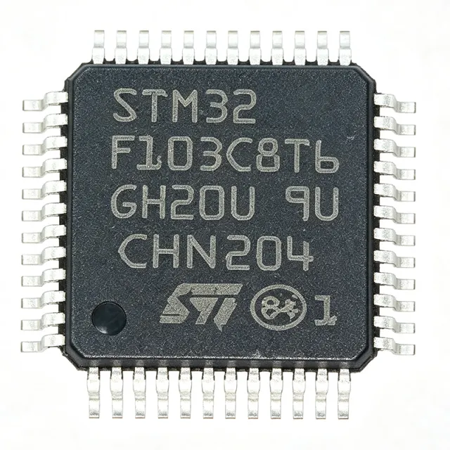
STM32F103C8T6 — 72 МГц MCU Cortex-M3, 64 КБ Flash, LQFP-48 | STMicroelectronics
Артикул: STM32F103C8T6 ✓ Активен| Кол-во | Цена за ед. | Итого |
|---|---|---|
| 1 | $3.1 | $3,10 |
| 10 | $2.78 | $27,80 |
| 100 | $2.45 | $245,00 |
| 500 | $2.18 | $1.090,00 |
| 1.000 | $1.92 | $1.920,00 |
| 3.000 | $1.68 | $5.040,00 |
STM32F103C8T6 Обзор
Микроконтроллер (MCU) ARM Cortex-M3 — это 32-битное RISC-ядро процессора, разработанное Arm Holdings для встраиваемых приложений, требующих детерминированной работы в реальном времени при низком энергопотреблении. Cortex-M3 находится в нижней части семейства Cortex-M (выше Cortex-M0/M0+ и ниже Cortex-M4/M7), а микроконтроллеры этой категории объединяют ядро процессора с внутрикристальной памятью, периферией и аналоговыми блоками в единую систему-на-кристалле. Семейство STM32F103 конкретно принадлежит к более широкой иерархии: ARM Cortex-M3 -> 32-битный MCU -> серия STM32F1 -> основное семейство STM32 -> микроконтроллеры STMicroelectronics -> полупроводники. Эта иерархия важна, поскольку она определяет инструментальную цепочку (Arm Cortex-M3 поддерживает стандартные потоки Arm Keil, IAR, GCC и STM32CubeIDE) и модель программирования периферии, используемую на всей платформе STM32.
Ключевые особенности включают 64 КБ встроенной Flash с возможностью чтения во время записи, 20 КБ SRAM, диапазон питания от 2,0 В до 3,6 В, внутренний RC-генератор 8 МГц с умножителем PLL до 72 МГц, два 12-битных АЦП (преобразование 1 мкс, до 16 каналов), семь 16-битных таймеров и контроллер USB 2.0 Full-Speed device/host/OTG. Коммуникационная периферия включает три USART, два SPI (18 Мбит/с), две шины I2C (400 кГц), один интерфейс CAN 2.0B и один порт USB Full-Speed. 48-выводной корпус LQFP предоставляет 37 выводов GPIO, толерантных к 5 В.
С архитектурной точки зрения ядро Cortex-M3 обеспечивает 1,25 Dhrystone MIPS на МГц, поддерживает набор инструкций Thumb-2 и включает вложенный векторный контроллер прерываний (NVIC) с настраиваемым приоритетом и аппаратной обработкой стека. Встроенный регулятор напряжения и сброс при пониженном напряжении (BOR) упрощают проектирование питания, а 4-байтовый резервный регистр с выводом обнаружения вскрытия поддерживает режимы RTC с батарейным резервом.
Типичные применения включают платы промышленного управления, приводы двигателей (дополнения BLDC/PMSM FOC), устройства USB HID/COM-порт, интерфейсы узлов CAN-шины и недорогие платформы разработки, такие как известная плата "Blue Pill".
При проектировании с этим устройством размещайте керамический конденсатор развязки 100 нФ как можно ближе к каждой паре выводов VDD/VDDA и предусмотрите для вывода NRST подтягивающий резистор 10 кОм и опциональную кнопку сброса. Убедитесь, что состояние вывода BOOT0 соответствует желаемой загрузочной памяти при каждом включении питания.
Эта страница обобщает дистрибьюторские цены, прямые аналоги (сначала варианты STM32F103 того же бренда, затем совместимые по выводам детали других брендов) и практические заметки по проектированию, которых нет в техническом описании производителя.
Аналоги без доработки для STM32F103C8T6 — тот же корпус, pin-to-pin совместимость. Компоненты в других корпусах, требующие переработки PCB, исключены.
Инструмент быстрого сравнения — выберите альтернативные компоненты для сравнения бок о бок:
STM32F103CBT6
✓ В наличии
$3.2 / шт.
Открыть даташит →STM32F030C8T6
✓ В наличии
$0.98 / шт.
Открыть даташит →STM32F103C8T7
📋 Справочный аналог (нет в каталоге)
GD32F103C8T6
📋 Справочный аналог (нет в каталоге)
APM32F103C8T6
📋 Справочный аналог (нет в каталоге)
STM32F103C8T6 Максимальные параметры и электрические характеристики
| Core Architecture | ARM Cortex-M3 (32-bit RISC) |
| Максимальная тактовая частота | 72 MHz |
| Flash Memory | 64 KB |
| SRAM | 20 KB |
| Supply Voltage (VDD) | 2.0 V to 3.6 V |
| Корпус | LQFP-48 (7x7 mm, 0.5 mm pitch) |
| GPIO Count | 37 |
| ADC | 2x 12-bit, 1 µs, up to 16 channels |
| Timers | 7x 16-bit (including 1x watchdog, 2x SysTick) |
| USART | 3 |
| SPI | 2 (18 Mbit/s) |
| I2C | 2 (400 kHz) |
| USB | 1x USB 2.0 Full-Speed device/host/OTG |
| CAN | 1x CAN 2.0B |
| Рабочая температура | -40 °C to +85 °C (industrial grade) |
| Статус RoHS | Compliant |
Конфигурация выводов STM32F103C8T6
| Контакт 1 | VBAT — Backup battery supply input |
| Контакт 2 | PC13 — GPIO PC13, anti-tamper (RTC) |
| Контакт 3 | PC14 — GPIO PC14 / OSC32_IN |
| Контакт 4 | PC15 — GPIO PC15 / OSC32_OUT |
| Контакт 5 | OSC_IN — HSE oscillator input |
| Контакт 6 | OSC_OUT — HSE oscillator output |
| Контакт 7 | NRST — Reset input, active-low |
| Контакт 8 | VSSA — Analog ground |
| Контакт 9 | VDDA — Analog supply (2.4 V - 3.6 V) |
| Контакт 10 | PA0 — GPIO PA0 / WKUP / ADC_IN0 / TIM2_CH1 |
| Контакт 11 | PA1 — GPIO PA1 / ADC_IN1 / TIM2_CH2 |
| Контакт 12 | PA2 — GPIO PA2 / USART2_TX / ADC_IN2 |
| Контакт 13 | PA3 — GPIO PA3 / USART2_RX / ADC_IN3 |
| Контакт 14 | PA4 — GPIO PA4 / SPI1_NSS / ADC_IN4 |
| Контакт 15 | PA5 — GPIO PA5 / SPI1_SCK / ADC_IN5 |
| Контакт 16 | PA6 — GPIO PA6 / SPI1_MISO / ADC_IN6 |
| Контакт 17 | PA7 — GPIO PA7 / SPI1_MOSI / ADC_IN7 |
| Контакт 18 | PB0 — GPIO PB0 / ADC_IN8 / TIM3_CH3 |
| Контакт 19 | PB1 — GPIO PB1 / ADC_IN9 / TIM3_CH4 |
| Контакт 20 | PB2 — GPIO PB2 / BOOT1 (also PB-BOOT input) |
| Контакт 21 | PB10 — GPIO PB10 / I2C2_SCL / USART3_TX |
| Контакт 22 | PB11 — GPIO PB11 / I2C2_SDA / USART3_RX |
| Контакт 23 | VSS_1 — Digital ground |
| Контакт 24 | VDD_1 — Digital supply (2.0 V - 3.6 V) |
| Контакт 25 | PB12 — GPIO PB12 / SPI2_NSS / CAN2_RX |
| Контакт 26 | PB13 — GPIO PB13 / SPI2_SCK / CAN2_TX / USB_DP pull-up |
| Контакт 27 | PB14 — GPIO PB14 / SPI2_MISO |
| Контакт 28 | PB15 — GPIO PB15 / SPI2_MOSI |
| Контакт 29 | PA8 — GPIO PA8 / USART1_CK / TIM1_CH1 |
| Контакт 30 | PA9 — GPIO PA9 / USART1_TX / TIM1_CH2 |
| Контакт 31 | PA10 — GPIO PA10 / USART1_RX / TIM1_CH3 |
| Контакт 32 | PA11 — GPIO PA11 / CAN1_RX / USBDM (USB data minus) |
| Контакт 33 | PA12 — GPIO PA12 / CAN1_TX / USBDP (USB data plus) |
| Контакт 34 | PA13 — GPIO PA13 / JTMS / SWDIO |
| Контакт 35 | VSS_2 — Digital ground |
| Контакт 36 | VDD_2 — Digital supply (2.0 V - 3.6 V) |
| Контакт 37 | PA14 — GPIO PA14 / JTCK / SWCLK |
| Контакт 38 | PA15 — GPIO PA15 / JTDI |
| Контакт 39 | PB3 — GPIO PB3 / JTDO / TRACESWO |
| Контакт 40 | PB4 — GPIO PB4 / JNTRST |
| Контакт 41 | PB5 — GPIO PB5 / I2C1_SMBAI |
| Контакт 42 | PB6 — GPIO PB6 / I2C1_SCL / TIM4_CH1 |
| Контакт 43 | PB7 — GPIO PB7 / I2C1_SDA / TIM4_CH2 |
| Контакт 44 | BOOT0 — Boot mode select (0 = Flash, 1 = System bootloader) |
| Контакт 45 | PB8 — GPIO PB8 / TIM4_CH3 |
| Контакт 46 | PB9 — GPIO PB9 / TIM4_CH4 |
| Контакт 47 | VSS_3 — Digital ground |
| Контакт 48 | VDD_3 — Digital supply (2.0 V - 3.6 V) |
Типичное применение
STM32F103C8T6 подходит для 6 применениеs: Industrial Control Boards, USB HID / Virtual COM Port Devices, BLDC / PMSM Motor Drives, CAN-Bus Node Interface, Low-Cost Development Platforms ("Blue Pill"), IoT Sensor / Smart Home Edge Nodes.
Industrial Control Boards
The STM32F103C8T6 fits industrial control boards because its 72 MHz Cortex-M3 core and 64 KB Flash comfortably handle Modbus RTU slave firmware, PID loop control, and user-interface logic on a single chip. The dual 12-bit ADCs (1 µs, up to 16 channels) sample 4-20 mA sensor inputs at the kHz rates typical of PLC analog modules, while the three USARTs (USART1/2/3) support simultaneous RS-232/RS-485 fieldbus and a debug console. The 2.0 V to 3.6 V supply range aligns with 3.3 V industrial backplanes, and the -40 °C to +85 °C operating temperature meets most cabinet-mounted equipment specs. On-board CAN 2.0B lets a single MCU handle both a sensor bus and an external CANopen master.
Рекомендуется
USB HID / Virtual COM Port Devices
The STM32F103C8T6's integrated USB 2.0 Full-Speed device controller (12 Mbit/s) makes it a natural fit for USB HID-class peripherals, virtual COM-port bridges, and CDC-MSC composite devices without external PHY hardware. The 72 MHz core and 20 KB SRAM execute the standard ST USB device library (and STM32CubeMX-generated middleware) with room left for application logic, while the 64 KB Flash fits typical HID report descriptors and command parsers. Its 2.0 V to 3.6 V rail tolerance lets designers tap the USB 5 V bus through an LDO and run the MCU from a single 3.3 V supply. Designers should add ESD protection (USBLC6-2SC6) and a 1.5 kΩ pull-up on the D+ line to the USB connector.
Рекомендуется
BLDC / PMSM Motor Drives
The STM32F103C8T6 is widely used in sensorless or hall-sensored BLDC and PMSM motor drives for low- to mid-power applications (fans, pumps, e-bike hubs). Its 72 MHz Cortex-M3 plus advanced timers (TIM1 with complementary PWM and dead-time insertion) generate the 6-step or space-vector PWM that drives a 3-phase inverter at up to tens of kHz switching. The two ADCs trigger from timer events to sample phase currents within the PWM cycle for low-latency commutation, and the quadrature encoder interface on TIM2 supports sensored FOC firmware patterns. CAN bus readiness lets the drive communicate with a central PLC, while the 2.0-3.6 V range accepts a wide range of bus-powered motor-control supplies.
Рекомендуется
CAN-Bus Node Interface
The STM32F103C8T6 is a battle-tested choice for CAN 2.0B node interfaces used in automotive body-electronics, industrial CANopen, and medical device buses. The bxCAN peripheral supports standard and extended frames with hardware filter banks and a 1 Mbit/s bit rate suitable for most fieldbus deployments. With 64 KB Flash the device holds small CANopen/CANFestival stacks and application logic, while three USARTs allow a companion GPS or HMI link. Operating temperature of -40 °C to +85 °C suits non-automotive nodes; designers needing AEC-Q100 should select the STM32F103C8T7 variant. Drop a 60 Ω termination resistor only on the bus ends and add a TJA1050 or TCAN332 transceiver externally.
Рекомендуется
Low-Cost Development Platforms ("Blue Pill")
The STM32F103C8T6 is the headline MCU of the iconic "Blue Pill" development board that became the de-facto entry ticket to ARM Cortex-M3 firmware development. Its 72 MHz core, 64 KB Flash, SWD debug pins, USB connector, and 48-pin LQFP form factor fit on a 53 x 23 mm PCB with a USB micro-B port, a 3.3 V LDO, a reset button, and boot-mode jumpers. Students and hobbyists target it with STM32CubeIDE, PlatformIO, and the Arduino STM32 core, and any prototype firmware written on the Blue Pill ports directly to custom hardware when the same MCU is kept on the production board. The LQFP-48 footprint is also shared by several GD32 and APM32 pin-compatibles, simplifying second sourcing for educational kits.
Рекомендуется
IoT Sensor / Smart Home Edge Nodes
The STM32F103C8T6 handles Smart Home and IoT edge nodes that need local sensor aggregation, BLE/Wi-Fi module handshaking, and OTA bootloading without committing to a high-cost M4-class part. Three USARTs (USART1/2/3) drive an ESP-01 Wi-Fi co-processor, a GPS module, and a debug console in parallel; two SPIs (up to 18 Mbit/s) talk to a LoRa SX1278 or a small TFT display; two I2C buses serve a BME280 environmental sensor and an OLED panel. The 12-bit ADC samples analog sensors such as soil-moisture probes, and the RTC plus 4-byte backup register keep a wall-clock time across deep-sleep cycles powered by a CR2032. The 2.0-3.6 V supply range supports direct lithium-ion battery operation via an LDO or buck.
Рекомендуется
Сводка рекомендуемых товаров
Справочные инженерные данные для STM32F103C8T6 — сравнение, рекомендации по проектированию и информация о соответствии.
Руководство по выбору
Сравнение с аналогами
| Параметр | Этот товар | STM32F103CBT6 | STM32F103C8T7 | GD32F103C8T6 | APM32F103C8T6 | STM32F030C8T6 |
|---|---|---|---|---|---|---|
| Brand | STMicroelectronics | STMicroelectronics | STMicroelectronics | GigaDevice | GigaDevice | STMicroelectronics |
| Package | LQFP-48 (7x7 mm) | LQFP-48 (7x7 mm) - same | LQFP-48 (7x7 mm) - same | LQFP-48 (7x7 mm) - same | LQFP-48 (7x7 mm) - same | LQFP-48 (7x7 mm) - same |
| Core | ARM Cortex-M3 | ARM Cortex-M3 | ARM Cortex-M3 | ARM Cortex-M3 | ARM Cortex-M3 | ARM Cortex-M0 (-1 class) |
| Max Clock | 72 MHz | 72 MHz | 72 MHz | 108 MHz (+50%) | 96 MHz (+33%) | 48 MHz (-33%) |
| Flash | 64 KB | 128 KB (+100%) | 64 KB | 64 KB | 64 KB | 64 KB |
| SRAM | 20 KB | 20 KB | 20 KB | 20 KB | 20 KB | 8 KB (-60%) |
| USB | USB 2.0 Full-Speed | USB 2.0 Full-Speed | USB 2.0 Full-Speed | USB 2.0 Full-Speed | USB 2.0 Full-Speed | No USB |
| CAN | 1x CAN 2.0B | 1x CAN 2.0B | 1x CAN 2.0B | 1x CAN 2.0B | 1x CAN 2.0B | No CAN |
| Automotive Grade | No (industrial -40/+85C) | No | Yes (AEC-Q100) | No | No | No |
Ключевые отличия
- Совместимый по выводам прямой аналог с удвоенной Flash в том же семействе (против STM32F103CBT6)
- Автомобильный температурный класс AEC-Q100 доступен на том же кристалле (против STM32F103C8T7)
- Ядро в два-четыре раза быстрее на том же корпусе LQFP-48 (против GD32F103C8T6)
Заметки по проектированию
Размещайте керамические конденсаторы развязки 100 нФ как можно ближе к каждой паре выводов VDD/VDDA (выводы 24, 36, 48 / 9), с хотя бы одним объемным конденсатором 4,7 мкФ на основной шине 3,3 В в пределах 20 мм. VDDA требует низкоимпедансного соединения; если основной источник 3,3 В шумный, вставьте ферритовую бусину между VDD и VDDA. Подключите VBAT к VDD, если резервная батарея не используется. Всегда удерживайте вывод BOOT0 низким при включении питания для загрузки по умолчанию из Flash.
Прокладывайте дорожки кварцевого резонатора HSE 8 МГц короткими и симметричными, размещая резонатор в пределах 5 мм от OSC_IN/OSC_OUT (выводы 5/6), а конденсаторы нагрузки (обычно 20-30 пФ) заземляйте прямо у корпуса резонатора. Держите USB D+/D- (PA11/PA12) согласованными по длине (целевая разница <2 мм) и размещайте подтягивающий резистор 1,5 кОм на D+ рядом с разъемом, а не со стороны MCU. Обеспечьте подтягивающий резистор 10 кОм на NRST и низкоимпедансный путь к GND через кнопку сброса.
При использовании CAN или USB добавьте массив TVS-диодов, например USBLC6-2SC6 или PESD1CAN, рядом с разъемом для соответствия IEC 61000-4-2 ±8 кВ воздушный разряд и ±4 кВ контактный разряд. Внутренний подтягивающий резистор на USB D+ (PA12) недостаточно силен для надежного перечисления; рекомендуется внешний резистор 1,5 кОм к 3,3 В. Терминация шины CAN должна использовать 120 Ом только на обоих концах, с сетью разделительных конденсаторов для подавления отводов в многоузловых жгутах.
Не оставляйте BOOT0 плавающим — шум на этом выводе во время включения питания будет периодически загружать MCU в системный загрузчик, и код приложения будет казаться отсутствующим. Три распространенные ошибки: (1) оставление VBAT плавающим вместо подключения к VDD, что заряжает внутренний диод и повреждает записи в резервный регистр; (2) использование PA13/PA14 как GPIO без отключения JTAG/SWD, поскольку JTAG по умолчанию использует эти выводы после сброса; (3) настройка скорости вывода GPIO на '50 МГц' на выводах I2C, что вызывает звон — всегда выбирайте '2 МГц' с открытым стоком и внешними подтягивающими резисторами.
Информация о соответствии
RoHS-compliant per ST product page; AEC-Q100 grade is a separate SKU (STM32F103C8T7). Halogen-free status not explicitly verified in the provided data and flagged as 'unknown'.







