STW11NK90Z - 900V N-Channel Power MOSFET | STMicroelectronics
Артикул: STW11NK90Z ✓ Активен| Кол-во | Цена за ед. | Итого |
|---|---|---|
| 1 | $4.5 | $4,50 |
| 10 | $4.05 | $40,50 |
| 100 | $3.6 | $360,00 |
| 500 | $3.15 | $1.575,00 |
| 1.000 | $2.7 | $2.700,00 |
STW11NK90Z Обзор
A Power MOSFET is a type of field-effect transistor designed to handle significant power levels. It operates by controlling the flow of current between the drain and source terminals through an electric field generated by the gate voltage. Power MOSFETs are essential components in power electronics, serving as switches in power supplies, motor drives, and inverters. They are part of the broader category of discrete semiconductors, which also includes diodes, thyristors, and IGBTs.
Key features of the STW11NK90Z include a high voltage rating of 900V, making it suitable for applications such as switch-mode power supplies (SMPS), power factor correction (PFC) circuits, and high-voltage DC-DC converters. The low on-resistance minimizes conduction losses, improving overall efficiency. The device also features a fast switching speed, which is critical for reducing switching losses in high-frequency applications.
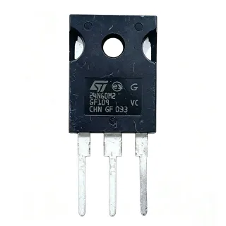
The STW11NK90Z utilizes STMicroelectronics' advanced PowerMESH technology, which provides a robust and reliable structure. The device has a maximum junction temperature of 150°C and is available in a TO-247 package, which offers a low thermal resistance of 0.5°C/W, enabling efficient heat dissipation. The device is RoHS compliant and lead-free, meeting environmental standards.
Typical applications include high-voltage power supplies, industrial motor drives, and renewable energy inverters. The device's high voltage rating and low on-resistance make it ideal for these applications, where efficiency and reliability are paramount.
When designing with the STW11NK90Z, it is important to consider the gate drive requirements. The device has a gate threshold voltage of 3V to 5V, and a gate charge of 45nC, which should be considered when designing the gate drive circuit. Additionally, proper heat sinking is essential to maintain the junction temperature within safe limits.
Аналоги без доработки для STW11NK90Z — тот же корпус, pin-to-pin совместимость. Компоненты в других корпусах, требующие переработки PCB, исключены.
Варианты в этой серии
Модели той же серии, совместимые без доработки с STW11NK90Z (тот же форм-фактор и посадочное место) — отличается по Package.
Инструмент быстрого сравнения — выберите альтернативные компоненты для сравнения бок о бок:
STW11NK90Z-1
✅ Прямая замена ⚠️ Характеристики не проверены📋 Справочный аналог (нет в каталоге)
STW11NK90Z-2
✅ Прямая замена ⚠️ Характеристики не проверены📋 Справочный аналог (нет в каталоге)
FCP11N90
✅ Прямая замена ⚠️ Характеристики не проверены📋 Справочный аналог (нет в каталоге)
IXFH11N90P
✅ Прямая замена ⚠️ Характеристики не проверены📋 Справочный аналог (нет в каталоге)
SPW11N90C3
✅ Прямая замена ⚠️ Характеристики не проверены📋 Справочный аналог (нет в каталоге)
STW11NK90Z Максимальные параметры и электрические характеристики
| Drain-Source Voltage (VDS) | 900 V |
| Continuous Drain Current (ID) at 25°C | 9.5 A |
| Continuous Drain Current (ID) at 100°C | 6 A |
| Pulsed Drain Current (IDM) | 38 A |
| Gate-Source Voltage (VGS) | ±30 V |
| On-Resistance (RDS(on)) | 0.85 ohm |
| Gate Threshold Voltage (VGS(th)) | 3 V to 5 V |
| Gate Charge (Qg) | 45 nC |
| Input Capacitance (Ciss) | 1900 pF |
| Output Capacitance (Coss) | 150 pF |
| Reverse Transfer Capacitance (Crss) | 20 pF |
| Maximum Power Dissipation (PD) | 250 W |
| Operating Junction Temperature (Tj) | -55°C to +150°C |
| Корпус | TO-247 |
| Тип монтажа | Through Hole |
| Статус RoHS | Compliant |
Конфигурация выводов STW11NK90Z
| Контакт 1 | Gate — Gate terminal for controlling the MOSFET |
| Контакт 2 | Drain — Drain terminal, connected to the load |
| Контакт 3 | Source — Source terminal, connected to ground |
Область безопасной работы
Типичное применение
STW11NK90Z подходит для 6 применениеs: Switch-Mode Power Supplies (SMPS), Power Factor Correction (PFC) Circuits, High-Voltage DC-DC Converters, Industrial Motor Drives, Renewable Energy Inverters, Lighting (HID and LED Drivers).
Switch-Mode Power Supplies (SMPS)
The STW11NK90Z is ideal for SMPS due to its high voltage rating (900V) and low on-resistance (0.85 ohm). In a typical flyback converter, the MOSFET switches at high frequency, and the low RDS(on) reduces conduction losses, improving efficiency. The fast switching speed minimizes switching losses, allowing higher operating frequencies and smaller magnetic components. The TO-247 package ensures adequate heat dissipation, which is critical for continuous operation at high power levels.
Рекомендуется
Power Factor Correction (PFC) Circuits
In PFC circuits, the STW11NK90Z is used as the boost switch to shape the input current waveform. Its high voltage rating (900V) handles the boosted voltage, while the low on-resistance minimizes conduction losses. The device's fast switching capability enables high-frequency operation, reducing the size of the boost inductor. The TO-247 package provides low thermal resistance, allowing the MOSFET to dissipate heat effectively during continuous operation.
Рекомендуется
High-Voltage DC-DC Converters
The STW11NK90Z is suitable for high-voltage DC-DC converters, such as those used in solar inverters and electric vehicle chargers. Its 900V drain-source voltage rating provides ample margin for high input voltages, and the low on-resistance ensures high efficiency. The fast switching speed reduces switching losses, enabling compact designs. The TO-247 package allows for efficient heat sinking, which is essential for high-power applications.
Рекомендуется
Industrial Motor Drives
In industrial motor drives, the STW11NK90Z is used in the inverter stage to switch DC to AC. Its high voltage rating (900V) is suitable for 3-phase AC motor drives operating from 400VAC or higher. The low on-resistance reduces conduction losses, improving overall drive efficiency. The device's ruggedness and thermal performance make it reliable for demanding industrial environments.
Рекомендуется
Renewable Energy Inverters
The STW11NK90Z is used in solar and wind inverters for DC-AC conversion. Its high voltage rating (900V) accommodates the high DC bus voltages in photovoltaic systems. The low on-resistance minimizes losses, maximizing energy harvest. The fast switching speed enables high-frequency PWM, improving output waveform quality. The TO-247 package ensures reliable thermal management in outdoor installations.
Рекомендуется
Lighting (HID and LED Drivers)
The STW11NK90Z can be used in high-intensity discharge (HID) lamp ballasts and high-power LED drivers. Its high voltage rating (900V) is suitable for AC mains applications, and the low on-resistance improves efficiency. The fast switching speed allows for compact magnetic components. The TO-247 package provides good thermal performance, ensuring long-term reliability.
Рекомендуется
Сводка рекомендуемых товаров
Справочные инженерные данные для STW11NK90Z — сравнение, рекомендации по проектированию и информация о соответствии.
Руководство по выбору
Сравнение с аналогами
| Параметр | Этот товар | STW11NK90Z-1 | FCP11N90 | IXFH11N90P | SPW11N90C3 |
|---|---|---|---|---|---|
| Package | TO-247 | TO-247-3 | TO-247 | TO-247 | TO-247 |
| Brand | STMicroelectronics | STMicroelectronics | onsemi | IXYS | Infineon |
| Drain-Source Voltage (VDS) | 900 V | 900 V | 900 V | 900 V | 900 V |
| Continuous Drain Current (ID) at 25°C | 9.5 A | 9.5 A | 11 A | 11 A | 11 A |
| On-Resistance (RDS(on)) | 0.85 ohm | 0.85 ohm | 0.75 ohm | 0.85 ohm | 0.75 ohm |
| Gate Charge (Qg) | 45 nC | 45 nC | 40 nC | 50 nC | 40 nC |
| Maximum Power Dissipation (PD) | 250 W | 250 W | 250 W | 250 W | 250 W |
| Operating Junction Temperature (Tj) | -55°C to +150°C | -55°C to +150°C | -55°C to +150°C | -55°C to +150°C | -55°C to +150°C |
Ключевые отличия
- High voltage rating of 900V (против FCP11N90)
- Low on-resistance of 0.85 ohm (против IXFH11N90P)
- Proven PowerMESH technology (против SPW11N90C3)
Заметки по проектированию
The STW11NK90Z has a maximum power dissipation of 250W. At high power levels, proper heat sinking is essential. The TO-247 package has a junction-to-case thermal resistance of 0.5°C/W. Use a heatsink with a thermal resistance of less than 0.5°C/W to keep the junction temperature below 150°C. For example, at 100W dissipation, the case temperature rise is 50°C, so the heatsink must maintain the case temperature below 100°C.
For the TO-247 package, ensure the mounting hole is properly sized and the leads are soldered with adequate thermal relief. Use a large copper area on the PCB connected to the drain tab for heat spreading. Place the gate drive components close to the gate pin to minimize parasitic inductance. Use a gate resistor (e.g., 10 ohm) to dampen oscillations.
Do not exceed the maximum gate-source voltage of ±30V. Ensure the gate drive voltage is within the recommended range (typically 10V to 15V) to fully enhance the channel. Avoid operating the device in the linear region for extended periods, as this can cause excessive power dissipation and thermal runaway. Use a proper snubber circuit to limit voltage spikes during switching.
Информация о соответствии
RoHS compliant per STMicroelectronics product page. Not AEC-Q101 qualified for automotive.