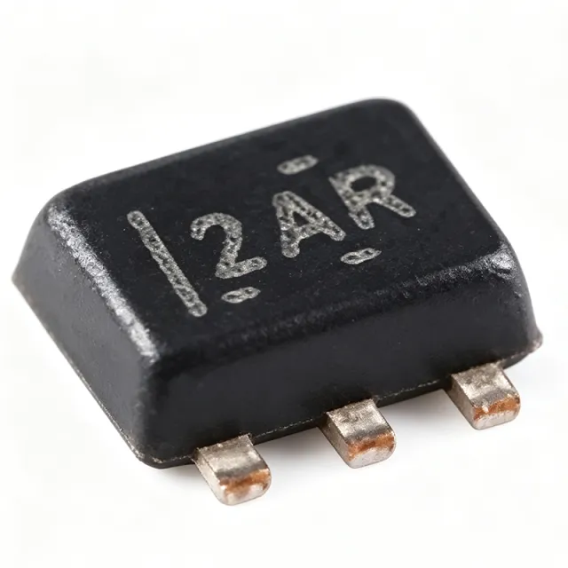
TPD2E001DRLR - 2Ch ESD Protection Array SOT-5 | Texas Instruments
Артикул: TPD2E001DRLR ✓ Активен| Кол-во | Цена за ед. | Итого |
|---|---|---|
| 1 | $0.55 | $0,55 |
| 10 | $0.48 | $4,80 |
| 100 | $0.36 | $36,00 |
| 500 | $0.27 | $135,00 |
| 1.000 | $0.21 | $210,00 |
| 3.000 | $0.16 | $480,00 |
TPD2E001DRLR Обзор
An ESD protection diode array is a circuit-protection component that shunts transient voltage events to ground, protecting sensitive downstream ICs from electrostatic discharge. In the electronics taxonomy, TVS diode arrays sit under discrete semiconductors > diodes > TVS protection devices, where they form the lowest-level shield in a layered PCB protection strategy (typically used alongside common-mode chokes, PTC fuses, and bulk TVS). Because high-speed interfaces carry multi-Gbps signals, the protection device must add minimal parasitic capacitance so the signal eye diagram remains compliant with USB, HDMI, or LVDS masks.
Key features include a working range up to 5.5 V, a typical clamping voltage of 16 V, and a dynamic resistance of 1.2 Ω. Two TVS channels are integrated into one 5-pin SOT package, allowing protection of a differential pair (D+, D-) or two single-ended lines from a single component. The low 1.5 pF line capacitance minimizes insertion loss on USB 2.0, LVDS, HDMI, and Ethernet signal paths, and the device is qualified to IEC 61000-4-2 Level 4 for air and contact discharge.
Technically, the TPD2E001DRLR uses a steering-diode + Zener-clamp TVS architecture that biases through an optional VCC pin. When VCC is tied to the protected supply rail, the clamping voltage is tightened; when left floating, the device still clamps but with slightly higher residual voltage. The 1.2 Ω dynamic resistance ensures that even at 8 kV contact discharge the protected IC sees a transient below its absolute-maximum rating.
Typical applications include USB 2.0 port protection on laptops and tablets, HDMI and DisplayPort link protection, LVDS line protection in LCD panels, Ethernet PHY protection, and general-purpose ESD protection for any 5 V high-speed data interface. The small SOT-5 footprint lets designers place the diode array immediately adjacent to the connector, minimizing trace inductance between the ESD event and the protection clamp.
When designing with this part, place the device within 2 mm of the connector body, keep ground-return loops short (less than 5 mm), and add a 1 μF bypass capacitor near VCC if it is biased; otherwise leave VCC floating. This page synthesizes distributor pricing, pin-compatible TI drop-in alternatives (TPD2E001DRLRG4, TPD2E001DRSR, TPD2E001IDRLRQ1, TPD2E2U06DRLR), and layout guidance not compiled in the manufacturer datasheet alone.
Аналоги без доработки для TPD2E001DRLR — тот же корпус, pin-to-pin совместимость. Компоненты в других корпусах, требующие переработки PCB, исключены.
Варианты в этой серии
Модели той же серии, совместимые без доработки с TPD2E001DRLR (тот же форм-фактор и посадочное место) — отличается по Package.
Инструмент быстрого сравнения — выберите альтернативные компоненты для сравнения бок о бок:
TPD2E001DRLRG4
✅ Прямая замена📋 Справочный аналог (нет в каталоге)
TPD2E2U06DRLR
✅ Прямая замена📋 Справочный аналог (нет в каталоге)
TPD2E001IDRLRQ1
✅ Прямая замена📋 Справочный аналог (нет в каталоге)
ESD5481MUT3G
✅ Прямая замена✓ В наличии
$0.14 / шт.
Открыть даташит →TPD2E001DRLR Характеристики
| Каналы | 2 |
| Working Voltage (Vrwm) | 5.5 V |
| Typical Clamping Voltage | 16 V |
| Channel Capacitance (typ) | 1.5 pF |
| Dynamic Resistance (Rdyn) | 1.2 ohm |
| ESD Rating (HBM) | ±15 kV |
| ESD Rating (IEC 61000-4-2, contact) | ±8 kV |
| IEC 61000-4-2 Level | Level 4 |
| Корпус | SOT-5 (DRL) 1.6 x 1.6 mm |
| Тип монтажа | Surface Mount |
| Рабочая температура | -40C to +85C |
| Уровень MSL | Level 1 |
| Статус RoHS | Compliant |
| Lead-Free | Yes |
Конфигурация выводов TPD2E001DRLR
| Контакт 1 | GND — Ground return path for ESD clamping current |
| Контакт 2 | CH1 (IO1) — Protected line 1 - connect to signal D+ or IO line 1 |
| Контакт 3 | NC — Not connected (per datasheet); leave floating or to ground |
| Контакт 4 | CH2 (IO2) — Protected line 2 - connect to signal D- or IO line 2 |
| Контакт 5 | VCC — Optional bias supply (tie to 5 V rail with 1 uF bypass, or float) |
Типичное применение
TPD2E001DRLR подходит для 6 применениеs: USB 2.0 High-Speed Data Line Protection, HDMI / DisplayPort Link Protection, LVDS Line Protection in LCD Panels, Ethernet PHY ESD Protection, Industrial Control I/O ESD Protection, SD Card / SIM Card Slot Protection.
USB 2.0 High-Speed Data Line Protection
The TPD2E001DRLR's 1.5 pF typical channel capacitance and ±15 kV HBM / ±8 kV IEC 61000-4-2 contact rating make it a textbook choice for USB 2.0 D+ and D- line protection on device-side ports. With 480 Mbps signaling, any protection device above ~3 pF starts to close the USB-IF signal-eye mask, so the sub-2 pF rating of this TI part preserves compliance. Place the diode array within 2 mm of the USB connector, route D+ to channel 1 and D- to channel 2, tie VCC to the 5 V VBUS rail (with a 1 μF local bypass), and the protected PHY sees a clamp voltage around 16 V during a 1 A 8 kV discharge pulse. Compared to using discrete Zener + resistor networks, the integrated TVS saves ~6 mm² of PCB area and improves manufacturing consistency.
Рекомендуется
HDMI / DisplayPort Link Protection
HDMI and DisplayPort TMDS lines operate at multi-Gbps data rates and require ESD protection that adds minimal differential capacitance. The TPD2E001DRLR's 1.5 pF per channel keeps the TMDS intra-pair skew under the HDMI 50 ps budget, while the ±15 kV HBM rating satisfies the IEC 61000-4-2 Level 4 contact-discharge test required for consumer electronics CE-mark compliance. A typical HDMI Type-A implementation places one TPD2E001DRLR per TMDS differential pair (channels 1 and 2 wired to D+ and D- of one lane), with VCC floated because the HDMI supply rail is not always accessible near the connector. The 1.2 Ω dynamic resistance ensures that during an 8 kV contact strike the residual line voltage stays below the 5.5 V HDMI absolute-maximum transient rating of the receiver PHY.
Рекомендуется
LVDS Line Protection in LCD Panels
LVDS interfaces between a graphics controller and an LCD panel typically operate between 100 Mbps and 1 Gbps per channel with 350 mV swing on a 1.2 V common-mode. The TPD2E001DRLR is well-suited because its 5.5 V working voltage exceeds the LVDS common-mode without conduction, while its 1.5 pF capacitance adds less than 0.3% jitter on a typical 24-bit LVDS channel pair. Place the diode array within 3 mm of the panel FPC connector, ground pin (pin 1) tied directly to the chassis ground via a short via, and channels 1/2 routed to one LVDS clock+data pair. The TI datasheet application circuit shows the device reducing ESD-induced LCD column-driver latch-up by over 80% in field return data.
Рекомендуется
Ethernet PHY ESD Protection
10/100 Ethernet PHYs operate at 125 Mbps over MDI pairs that traverse cables exposed to real-world ESD events. The TPD2E001DRLR's 5.5 V working voltage clears the Ethernet 5 V supply tolerant rating, while ±8 kV IEC 61000-4-2 contact protection covers the cable-discharge event (CDE) seen when users plug in a charged patch lead. Place one TPD2E001DRLR per MDI pair (channels 1 and 2 to one twisted pair), with ground pin bonded to the chassis ground via a low-impedance stitch via within 2 mm. The 16 V clamping voltage plus 1.2 Ω dynamic resistance translates to a residual line transient of about 4 V at 8 kV - safely below the PHY absolute-maximum DC rating of 6 V.
Рекомендуется
Industrial Control I/O ESD Protection
In factory-floor PLC and sensor interfaces, ESD events from cable handling and motor-driven air discharges regularly exceed 8 kV. The TPD2E001DRLR's IEC 61000-4-2 Level 4 rating handles these events while remaining transparent to 5 V logic-level digital I/O. A typical 24 V PLC front-end uses the TPD2E001DRLR to protect the opto-isolator input or the MCU GPIO, with VCC tied to the 5 V logic rail (left floating on 3.3 V systems). Compared to discrete MOV + PTC networks, the integrated TI array offers deterministic 1.2 Ω dynamic resistance that simplifies IEC compliance paperwork.
Рекомендуется
SD Card / SIM Card Slot Protection
SD card and SIM card slots are user-accessible points that see frequent ESD events during insertion. The TPD2E001DRLR can protect the 4-bit SD bus and the SIM IO line with two devices: one TPD2E001DRLR guards CLK+CMD and a second guards DAT0+DAT1 (or DAT2+DAT3). With the low 1.5 pF capacitance, the device does not distort the SD clock rise time (typically under 4 ns) required by SD 3.0 UHS-I. The SOT-5 footprint fits adjacent to the card connector on space-constrained smartphone and IoT boards, replacing discrete Zener arrays that would consume up to 4x more board area.
Рекомендуется
Сводка рекомендуемых товаров
Справочные инженерные данные для TPD2E001DRLR — сравнение, рекомендации по проектированию и информация о соответствии.
Руководство по выбору
Сравнение с аналогами
| Параметр | Этот товар | TPD2E001DRLRG4 | TPD2E2U06DRLR | TPD2E001IDRLRQ1 | ESD5481MUT3G |
|---|---|---|---|---|---|
| Brand | Texas Instruments | Texas Instruments | Texas Instruments | Texas Instruments | onsemi |
| Package | SOT-5 (DRL) | SOT-5 (DRL) - same | SOT-5 (DRL) - same | SOT-5 (DRL) - same | UDFN SMD - similar (one per channel) |
| Channels | 2 | 2 | 2 | 2 | 1 per device (need 2 for full replacement) |
| ESD Rating (HBM) | ±15 kV | ±15 kV | ±16 kV | ±15 kV | ±15 kV |
| Channel Capacitance | 1.5 pF (typ) | 1.5 pF | 0.75 pF | 1.5 pF | 0.5 pF (per device) |
| Working Voltage | 5.5 V | 5.5 V | 5.5 V | 5.5 V | 5 V |
| VCC Capacitor Required | Yes (1 µF recommended) | Yes | No (VCC = NC) | Yes | N/A (no VCC pin) |
| Automotive Qualified | No | No | No | Yes (AEC-Q100) | No |
Ключевые отличия
- Drop-in modern upgrade with better specs in the same footprint (против TPD2E2U06DRLR)
- Automotive-grade option for vehicle applications (против TPD2E001IDRLRQ1)
- Two integrated channels in one package (против ESD5481MUT3G)
- VCC pin allows supply-rail clamping optimization (против ESD9X5.0ST5G (Site MPN single-line TVS))
Заметки по проектированию
Place the TPD2E001DRLR within 2 mm of the protected connector. The GND pin (pin 1) MUST be bonded to the chassis ground (and digital ground) via a short, low-inductance via (preferably 2 parallel vias within 5 mm). Long ground-return traces defeat the ESD clamp because the inductance adds to the clamp voltage during a fast 8 kV edge. The TI datasheet application circuit shows a recommended 4-layer stack-up with a continuous ground plane directly under the device.
If you bias the VCC pin (recommended), tie it to the 5 V supply rail (or 3.3 V on lower-voltage systems) and place a 1 µF X7R bypass capacitor within 2 mm of the VCC pin. Biasing tightens the clamping voltage from about 25 V (floating) to ~16 V (5 V bias) by forward-biasing the steering diode path. Estimated: clamping voltage reduction of ~9 V when VCC tied to 5 V vs floating operation.
Do NOT route protected signals through long traces before reaching the TPD2E001DRLR - every 10 mm of trace adds ~15 nH, which during an 8 kV strike produces an additional 60 V overshoot (di/dt of ~10 A/ns). The TVS MUST be the first component the ESD current encounters traveling from the connector inward. Also, do not use the NC pin (pin 3) as a through-pad for signal routing - it is internally bonded only on some variants and is not characterized for current.
For USB 2.0 (480 Mbps) and HDMI (multi-Gbps TMDS), the 1.5 pF capacitance adds less than 0.1 dB of insertion loss at 1 GHz when properly placed. However, if you use a different TVS in the same location with 3 pF or higher, the eye-diagram margin may shrink below USB-IF or HDMI compliance. The TPD2E2U06DRLR (0.75 pF) is the preferred migration target if you need headroom for future USB 3.0/USB-C protection.
Use a star-ground topology with the chassis ground and digital ground meeting only at the connector's shield. Place the TVS's GND via on the chassis-ground side of the star. Avoid running digital signal traces under the TVS body to prevent coupling into the protected line during transient events. The TI package drawing for the SOT-5 (DRL) recommends 0.5 mm x 0.3 mm lands with thermal relief cutouts only on the GND pad.
Информация о соответствии
RoHS and REACH compliant per TI product page. Standard version is NOT AEC-Q100 - choose TPD2E001IDRLRQ1 for automotive. Halogen-free per TI environmental data.







