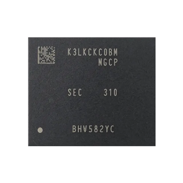
What is the SK Hynix H5ANAG6NCMR-XNC?
The SK hynix H5ANAG6NCMR-XNC is a 16Gb DDR4 SDRAM organized as 1G x 16, with a verified data rate of 3200 Mbps/pin, a 1.2 V supply, and a surface-mount FBGA-96 package. It uses CMOS technology and the XN 3200 speed grade. The component is active and RoHS compliant, with 13,000 units listed in stock and a minimum order quantity of one. Verified pricing starts at $163.125 for one unit, decreases through the volume tiers, and reaches $95.1563 at 1,000 units as of 2026-11-01. These specifications make the device a practical candidate for DDR4-3200 main-memory, embedded-computing, networking, server-module, graphics, and data-acquisition designs. Review the H5ANAG6NCMR-XNC product page for current sourcing information.
Takeaway: Select the H5ANAG6NCMR-XNC when the design needs 16Gb of DDR4 storage, a wide x16 interface, 3200 Mbps/pin operation, and a 1.2 V supply.
How do you select and design in the H5ANAG6NCMR-XNC?
Start with controller compatibility. The memory controller must support DDR4-3200 operation and the timing requirements associated with the XN speed grade. The device provides a 16-bit data path, so a single device supports a 16-bit channel, while two devices provide a 32-bit channel. For conventional 64-bit memory subsystems, the application data identifies eight x16 devices as one option for a 16 GB DIMM-class arrangement. A controller that specifically expects x8 devices requires a different organization and cannot be populated with this part without changing the memory topology.
The basic verified specifications are:
| Parameter | Verified value | Design implication |
|---|---|---|
| Memory type | DDR4 SDRAM, volatile DRAM | Volatile system memory requiring periodic refresh |
| Memory size | 16Gb | 2 GB of storage per device |
| Organization | 1G x 16 | 16-bit-wide data interface |
| Data rate | 3200 Mbps/pin | DDR4-3200 controller support required |
| Supply voltage | 1.2 V | Plan a dedicated 1.2 V memory rail |
| Technology | CMOS | Synchronous DRAM operation |
| Power class | Normal Power | Use the normal-power classification in power planning |
| Interface | Parallel | Controller and PCB routing must support a parallel DDR4 interface |
| Speed grade | XN, 3200 | Validate against the controller timing table |
| Package | FBGA-96 | Requires a corresponding surface-mount land pattern and assembly process |
| Mounting type | Surface mount | Designed for PCB assembly rather than through-hole insertion |
| Product status | Active | Current product status in the XAIPART database |
| RoHS status | RoHS Compliant | Supports RoHS-compliant sourcing requirements |
Takeaway: Validate three items before committing the footprint: DDR4-3200 controller support, the required x16 channel population, and the 1.2 V power-delivery design.
How should the memory channel be sized?
For a compact 32-bit subsystem, two H5ANAG6NCMR-XNC devices provide 32 Gb of total memory, equal to 4 GB. Their combined data width is 32 bits because each device has a 16-bit organization. This configuration is relevant to embedded boards and FPGA-based systems that need more capacity or bandwidth than a single x16 device provides without moving to a wider controller population.
The verified application data also describes an eight-device arrangement for a 64-bit, 16 GB DIMM-class subsystem. That calculation follows directly from the device specifications: eight devices multiplied by 16Gb equals 128Gb, or 16 GB, and eight 16-bit data paths provide 64 aggregate data bits. These are topology calculations only; the complete memory interface still depends on the controller, module organization, routing, and timing configuration.
| Configuration | Calculated capacity | Calculated data width | Verified use case |
|---|---|---|---|
| 1 device | 16 Gb, or 2 GB | 16 bits | Compact 16-bit memory subsystem |
| 2 devices | 32 Gb, or 4 GB | 32 bits | Embedded or controller-based 32-bit channel |
| 8 devices | 128 Gb, or 16 GB | 64 bits | DIMM-class subsystem |
Do not select this x16 device solely from total capacity. The controller's expected organization and the PCB's topology determine whether x16, x8, or a mixed population is appropriate. The supplied comparison specifically warns that x16 and x8 parts with similar density and speed are not interchangeable for the same bus without checking the controller requirements.
Takeaway: Size the channel from both capacity and organization; 16Gb density does not make an x16 device a substitute for an x8 device.
How should the 1.2 V rail and signal integrity be handled?
Plan the memory subsystem around a 1.2 V VDD rail. The supplied design guidance calls for fly-by routing, on-die termination, and power delivery that follows the applicable DDR4 layout practice. It also identifies write leveling, a low-jitter clock, and controller timing-table verification as checks for designs operating at 3200 Mbps.
Because FBGA-96 is a fine-pitch surface-mount package, assembly and layout quality directly affect the implementation. Confirm that the PCB land pattern, paste stencil, reflow profile, and board-level power distribution are prepared for FBGA-96. The verified package data does not include a package diagram, pin table, or MSL rating, so this article does not reproduce those details. Obtain the complete family documentation and the product-page data before releasing a production layout.
For embedded systems, the application data recommends confirming the device temperature grade against ambient requirements and using an appropriate family variant when an extended industrial-temperature range is mandatory. Because the operating-temperature range is not stated in the supplied component record, engineers should not infer it from the XN suffix. Make the grade check a formal sourcing condition.
Takeaway: Treat the DDR4 interface as a complete signal-integrity and power-design problem; the 3200 Mbps grade alone does not establish layout compliance.
How do price and inventory change the sourcing decision?
Use the verified price tiers as the current sourcing baseline as of 2026-11-01:
| Order quantity | Verified unit price |
|---|---|
| 1 or more | $163.125 |
| 10 or more | $117.8125 |
| 100 or more | $104.2187 |
| 500 or more | $99.6875 |
| 1,000 or more | $95.1563 |
The database also contains an older FAQ price of approximately $41.87 as of 2026-09-05. That figure conflicts with the newer tier table dated 2026-11-01. Use the later tier table for planning and request a live quote before placing an order.
Takeaway: The current verified tiers materially reduce unit cost at higher quantities, but production commitments should use a confirmed quote rather than the older FAQ price.
Which alternatives and comparisons are available for the H5ANAG6NCMR-XNC?
The supplied alternatives data provides one named family comparison: the SK hynix H5ANAG6NDMR-VKC. Both devices are 16Gb DDR4 SDRAMs with x16 organization, but their suffix and die information differ. The H5ANAG6NCMR-XNC uses the XN 3200 grade and CMR die revision, while the H5ANAG6NDMR-VKC uses the VK speed grade and a newer DMR die revision. The comparison data states that the two parts share all key parameters, but it does not provide the VK data rate, package, or timing values. Therefore, the available record does not establish unconditional drop-in interchangeability.
| Parameter | H5ANAG6NCMR-XNC | H5ANAG6NDMR-VKC | Selection consequence |
|---|---|---|---|
| Manufacturer | SK hynix | SK hynix | Same manufacturer |
| Memory type | DDR4 SDRAM | DDR4 SDRAM | Same memory technology |
| Memory size | 16Gb | 16Gb | Same verified density |
| Organization | 1G x 16 | 16Gb x16 | Same x16 organization |
| Speed grade | XN, 3200 | VK | Do not infer the VK rate from the XN device |
| Die revision | CMR | Newer DMR | Verify the timing and compatibility implications |
| Package | FBGA-96 | Not separately specified in the supplied comparison | Confirm the physical footprint before substitution |
The alternative is best treated as a qualified second-source candidate, not an automatic drop-in replacement. Before substituting it, request a live quotation, confirm the FBGA-96 footprint, validate the memory-controller timing table against the VK grade, and verify all operating requirements in the approved source data. The broader XAIPART component catalog can support additional sourcing searches, but components not documented in the supplied comparison are not presented as verified alternatives here.
Takeaway: H5ANAG6NDMR-VKC is the only named alternative with supplied data; qualify its VK speed grade and physical package before treating it as interchangeable.
What does the lifecycle and stock position mean for buyers?
The H5ANAG6NCMR-XNC has an active product status, and the XAIPART record lists 13,000 units in stock with an MOQ of one. This supports prototype purchasing, incremental production, and consolidated procurement without a large initial commitment. The active designation indicates that the part remains marketed as a current product in the supplied database; it does not provide a scheduled end-of-life date or a guaranteed future allocation.
Supply conditions can differ by channel. The supplied FAQ references a distributor listing of five pieces, while the current product record reports 13,000 units. These figures describe different availability snapshots and should not be combined into one distributor count. Request a live quote to confirm the amount available, traceability, lead time, and date code before binding a production schedule. The XAIPART Blog provides related sourcing and component-selection context, while the live product record remains the correct place to confirm the orderable quantity.
Because the part is active, RoHS compliant, and stocked, the immediate sourcing risk appears lower than for a component with an inactive lifecycle status or limited inventory. That conclusion does not eliminate normal memory-market risk: prices and inventory can move quickly, so a purchase order should be based on current commercial confirmation rather than this static record alone.
Takeaway: The present record supports active procurement, but reserve production supply against a current quote and confirmed lead time.
What should buyers watch in the H5ANAG6NCMR-XNC roadmap?
The first design watchpoint is density per device. At 16Gb, the H5ANAG6NCMR-XNC provides 2 GB in one x16 package. That capacity supports compact embedded systems, two-device 32-bit channels, and larger DIMM-class populations without increasing the device count as much as a lower-density alternative would. For cost-constrained designs, compare the quantity break price with the cost and routing burden of populating more devices.
The second watchpoint is the 3200 Mbps/pin data rate. The XN grade makes the component relevant to controllers specified for DDR4-3200, but every new controller qualification should include timing, write leveling, termination, and layout validation. Engineers following higher-bandwidth system discussions can use the article on bandwidth cuts and sourcing questions as broader context, while treating this component's verified 3200 Mbps/pin limit as the controlling specification.
The third watchpoint is power density. The verified 1.2 V operating requirement reduces the memory rail voltage relative to the supplied DDR3 comparison in the product description, while the normal-power classification provides a defined power category. The design should still include a dedicated low-voltage rail, local decoupling, and current-budget checks appropriate to the number of populated devices. For acquisition systems, the application guidance also recommends isolating DRAM ground currents from sensitive analog references.
The fourth watchpoint is package consolidation. FBGA-96 supports high component density, but it requires disciplined PCB layout and specialized assembly. High-volume designs should test package assembly capability, inspect solder joints, and verify the programmed interface configuration on assembled hardware. The article on sustained-write capture workflows offers adjacent context for memory-intensive data systems, but the H5ANAG6NCMR-XNC remains a volatile DDR4 SDRAM rather than a nonvolatile storage device.
Finally, monitor lifecycle and inventory at each design revision. The current position—active status, 13,000 units, and an MOQ of one—is favorable for current sourcing, but neither inventory nor price remains fixed. Track the exact MPN, 16Gb x16 organization, XN speed grade, 1.2 V supply, and FBGA-96 package rather than accepting a generic DDR4 substitute. This makes the design resilient to part-number changes, price movement, and second-source qualification.
Takeaway: Buyers should watch density, controller timing, 1.2 V power delivery, FBGA assembly maturity, and live inventory while preserving the verified configuration.
Mga Komento
Maging kauna-unahang nagsasalita ng komento.
🔐 Mangyaring mag-sign in upang mag-post ng comment.
Wala kang account? Mag-sign up