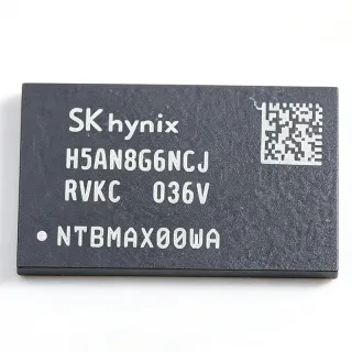
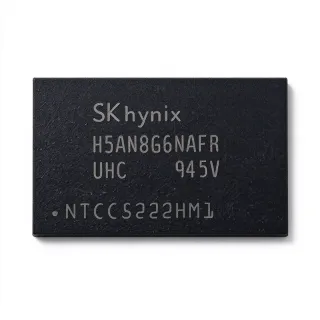
H5ANAG6NCMR-XNC - 16Gb DDR4 SDRAM x16 FBGA-96 | SK Hynix
MPN: H5ANAG6NCMR-XNC ✓ Active| Qty | Unit Price | Extended |
|---|---|---|
| 1 | $41.87 | $41.87 |
| 10 | $39.78 | $397.80 |
| 100 | $36.63 | $3,663.00 |
| 500 | $33.5 | $16,750.00 |
| 1,000 | $31.4 | $31,400.00 |
H5ANAG6NCMR-XNC Overview
DDR4 SDRAM (Double Data Rate 4 Synchronous Dynamic Random Access Memory) is the fourth generation of the DDR DRAM family, a class of volatile memory that transfers data on both clock edges and synchronizes operation to a system clock. Within the memory hierarchy, DDR4 SDRAM sits below DDR5 and above DDR3, and serves as main memory in the broader power and data management IC ecosystem for computing systems.
Key features of the H5ANAG6NCMR-XNC include its large 16Gb density organized as 1G words of 16 bits, a 3200 Mbps/pin transfer rate suitable for high-bandwidth main memory, a low 1.2V operating voltage that reduces dynamic power versus DDR3, and the space-saving FBGA (Fine-Pitch Ball Grid Array) package. The XN speed bin designation indicates the 3200 Mbps grade; the CMR suffix denotes standard CMOS DRAM process.
Technically, DDR4 SDRAMs like this device use an 8n prefetch architecture, bank groups, and programmable CAS latency to sustain high effective bandwidth while managing access latency. Per SK hynix product documentation, the H5ANAG6NCMR family is ideally suited for main memory applications that require large memory density and high bandwidth, with normal power classification and 1.2V operation.
Typical applications include desktop and notebook PC main memory modules, servers and embedded computing boards, industrial controllers requiring large volatile storage, and networking equipment data buffers.
When designing with this device, ensure the memory controller supports DDR4-3200 timing and that fly-by routing, on-die termination, and power delivery for the 1.2V VDD rail follow JEDEC DDR4 layout practice.
This page synthesizes distributor pricing, drop-in alternatives, and practical design notes not found in the manufacturer datasheet.
Drop-in alternatives for H5ANAG6NCMR-XNC — same package, pin-to-pin compatible. Different-package parts requiring PCB rework are excluded.
Variants in this series
Same-series models that are drop-in compatible with H5ANAG6NCMR-XNC (same form factor and footprint) — differing in Package, Interface, Data Rate, Mounting Type, Memory Size.
Quick Comparison Tool — Select alternative parts for side-by-side comparison:
H5ANAG6NCR-VKC
✅ Drop-In✓ In Stock
Contact for price
View Datasheet →H5ANAG6NCR-UHC
✅ Drop-In✓ In Stock
$9.2 / Unit
View Datasheet →H5ANAG6NCR-RDC
✅ Drop-In✓ In Stock
$72.1 / Unit
View Datasheet →H5ANAG6NCJR-XNC
✅ Drop-In✓ In Stock
$84.97 / Unit
View Datasheet →H5ANAG6NAMR-UHC
✅ Drop-In✓ In Stock
$4.5 / Unit
View Datasheet →H5ANAG6NDMR-VKC
✅ Drop-In📋 Reference alternative (not in catalog)
MT40A1G16TD-062E
✅ Drop-In✓ In Stock
$18.41 / Unit
View Datasheet →H5ANAG6NCMR-XNC Maximum Ratings & Electrical Characteristics
| Memory Type | DDR4 SDRAM (Volatile DRAM) |
| Memory Size | 16 Gb |
| Memory Organization | 1G x 16 |
| Data Rate | 3200 Mbps/pin |
| Supply Voltage (VDD) | 1.2 V |
| Technology | CMOS |
| Power Class | Normal Power |
| Interface | Parallel |
| Speed Grade | XN (3200) |
| Package | FBGA-96 |
| Mounting Type | Surface Mount |
| Product Status | Active |
| RoHS Status | RoHS Compliant |
H5ANAG6NCMR-XNC fbga-96 Pin Configuration Guide
Pin configuration for H5ANAG6NCMR-XNC (fbga-96 package). This digital IC includes GPIO, communication interfaces (UART, SPI, I2C), and power pins. Refer to the manufacturer datasheet for alternate pin functions and configuration options. Essential for embedded system design and PCB layout.

No detailed pinout data available for H5ANAG6NCMR-XNC.
Refer to the datasheet for full pin configuration.
Typical Applications
H5ANAG6NCMR-XNC is suitable for 6 applications: Desktop and Notebook PC Main Memory, Embedded Computing and Industrial Controllers, Networking and Communication Equipment, Server Memory Modules, Graphics and Video Processing Boards, Test, Measurement, and Data Acquisition Systems.
Desktop and Notebook PC Main Memory
The H5ANAG6NCMR-XNC provides 16Gb of DDR4 main memory per device at a 3200 Mbps data rate, matching the bandwidth of mainstream Intel and AMD DDR4-3200 memory controllers. Its x16 organization lets a two-chip design deliver a 32-bit bus with 4 GB capacity, and eight devices build a full 64-bit, 16 GB DIMM-class subsystem. Because it operates from a 1.2V rail, dynamic power stays well below equivalent DDR3 densities at the same bandwidth. Place devices on fly-by-routed address/command lines with on-die termination enabled and verify SPD or controller timing tables against the XN speed bin.
Recommended
Embedded Computing and Industrial Controllers
Embedded x86 and ARM platforms that need large volatile memory benefit from the H5ANAG6NCMR-XNC density of 16Gb (2 GB) in a single 96-ball FBGA, minimizing board area versus stacking multiple 8Gb parts. The 3200 Mbps rate matches the DDR4-3200 interfaces of industrial SoCs and SoC-FPGA devices, sustaining high throughput for data logging and protocol processing. The 1.2V VDD rail simplifies power tree design alongside 5V/3.3V industrial I/O. Designers should confirm the commercial temperature suffix against ambient conditions and select an IT-grade variant of the family where -40C to +85C operation is mandatory.
Recommended
Networking and Communication Equipment
Routers, switches, and network processing cards use large DRAM buffers for packet queuing and deep-flow analysis. The H5ANAG6NCMR-XNC delivers 2 GB per device with DDR4-3200 bandwidth, allowing buffer depths that absorb microbursts without dropping to slower storage. Its x16 organization suits compact line-card memory subsystems where PCB layers are constrained, and FBGA-96 balls simplify BGA rework compared with stacked-package alternatives. Pair with a low-jitter clock source and series-damped fly-by routing; enable ODT and verify write leveling at 3200 Mbps to meet signal integrity margins on 8-layer boards.
Recommended
Server Memory Modules
Server RDIMMs and ECC UDIMMs built around 16Gb x16 devices such as the H5ANAG6NCMR-XNC achieve high capacity per rank while keeping device count low. For 72-bit ECC configurations, designers typically prefer x8 parts, but x16 devices serve cost-optimized servers and storage controllers where one rank of two x16 devices provides a 32-bit data path. The 3200 Mbps XN bin supports modern server memory clocks, and the normal-power classification keeps idle current predictable for data center thermal budgets. Confirm controller ECC logic compatibility since x16 devices use on-die ECC rather than side-band ECC.
Recommended
Graphics and Video Processing Boards
Frame buffers and video processing cards require high-bandwidth DRAM for 4K and multi-display pipelines. The H5ANAG6NCMR-XNC 16Gb density supports multi-frame buffering at high resolutions, and its 3200 Mbps/pin rate provides substantial read bandwidth for display controllers and video codecs. x16 organization reduces chip count versus x8 in 32-bit and 64-bit local buses common on FPGA-based video platforms. For deterministic video latency, tune the controller to limit bank-group conflicts and use the programmable CAS latency of the DDR4-3200 bin; validate refresh tREFI scheduling against frame deadlines.
Recommended
Test, Measurement, and Data Acquisition Systems
High-speed oscilloscopes, logic analyzers, and data acquisition platforms stream acquired samples into large DRAM capture buffers. The H5ANAG6NCMR-XNC offers 2 GB per device, extending capture depth, while DDR4-3200 bandwidth sustains sustained write rates from ADC front ends when access is organized in sequential bursts. The 96-ball FBGA supports compact memory daughtercards, and the 1.2V rail integrates cleanly with low-noise analog power schemes through a dedicated point-of-load regulator. Designers should isolate DRAM ground currents from analog references and verify burst-write throughput against the acquisition engine peak rate.
Recommended
Recommended Products Summary
Engineering reference data for H5ANAG6NCMR-XNC — comparison, design guidance, and compliance information.
Selection Guide
Comparison with Alternatives
| Parameter | This Product | H5ANAG6NCR-VKC | H5ANAG6NCR-UHC | H5ANAG6NDMR-VKC | MT40A1G16TD-062E |
|---|---|---|---|---|---|
| Package | FBGA-96 | FBGA-96 - same | FBGA-96 - same | FBGA-96 - same | FBGA-96 - same |
| Brand | SK Hynix | SK Hynix | SK Hynix | SK Hynix | Micron Technology |
| Memory Size | 16 Gb | 16 Gb | 16 Gb | 16 Gb | 16 Gb |
| Organization | 1G x 16 | 1G x 16 | 1G x 16 | 1G x 16 | 1G x 16 |
| Supply Voltage | 1.2 V | 1.2 V | 1.2 V | 1.2 V | 1.2 V |
| Technology | CMOS DDR4 | CMOS DDR4 | CMOS DDR4 | CMOS DDR4 (DMR die revision) | CMOS DDR4 |
| RoHS Status | Compliant | Compliant | Compliant | Compliant | Compliant |
| Lifecycle Status | Active | Active | Active | Active | Active |
Key Differentiators
- Top DDR4-3200 speed bin (XN) (vs H5ANAG6NCR-UHC)
- x16 organization minimizes device count (vs H5ANAG8NCMR-XNI)
- Cross-brand second source availability (vs MT40A1G16TD-062E)
Design Notes
At the 3200 Mbps data rate of the H5ANAG6NCMR-XNC, DDR4 fly-by routing of address/command/control lines is effectively mandatory. Match trace lengths within the group, use 40-ohm or 50-ohm controlled impedance, and enable write leveling plus read training in the memory controller. Keep data strobe pairs (DQS/DQS#) tightly length-matched to their associated DQ bits, and simulate the FBGA-96 ball escape pattern with IBIS models from SK hynix before committing to an 8-layer stackup.
The device operates from a 1.2V VDD rail with separate VDDQ termination provisions typical of DDR4. Size the point-of-load regulator for peak burst currents plus termination power; on a 64-bit bus of multiple devices, VTT termination current can reach several amps during simultaneous access. Use a dedicated VTT terminating regulator with tracking output and bulk capacitance near each device. Decouple each FBGA power ball with at least one 0.1 uF ceramic plus local bulk capacitance, per SK hynix DDR4 design guidelines.
The XN suffix encodes the DDR4-3200 speed grade - do not assume lower-bin compatibility, and confirm your controller timing table supports CL settings of this bin. Also verify temperature grade: standard-grade suffixes may not cover -40C ambient industrial requirements, in which case select the IT-grade variant of the 16Gb family. When second-sourcing to Micron MT40A1G16TD-062E, re-run memory training and recheck vendor-specific mode registers, since register maps differ between SK hynix and Micron dies.
Compliance Information
RoHS compliant per JLCPCB and Lisleapex distributor listings. REACH, halogen-free, and conflict minerals declarations were not stated in the provided source data.