ADC/DAC
Mga Produkto (2,700+)

ADC0801S040TS/C1:1 - 8-bit, 40MSPS Video ADC | NXP | 20-SSOP
The NXP ADC0801S040TS/C1:1 is an 8-bit universal analog-to-digital converter (ADC) optimized for video and general-purpose high-speed sampling applications, housed in a 20-pin LSSOP (TSSOP-equivalent) package. The device samples at up to 40 MSPS and accepts analog input signals in the 2.7 V to 5.5 V range, converting them into 8-bit parallel binary-coded digital words. According to the manufacturer datasheet, the converter uses a successive-approximation (SAR) architecture with an internal reference and supports CMOS/TTL-compatible digital I/O. An analog-to-digital converter is a semiconductor device that converts continuous analog signals into discrete digital codes for processing by microcontrollers, DSPs, FPGAs, or display pipelines. Within the broader signal-chain hierarchy, the ADC0801S040 belongs to the SAR-ADC family (Successive-Approximation Register ADC) -> ADC -> data converter -> mixed-signal IC -> integrated circuit. SAR ADCs deliver deterministic latency, single-cycle conversion, and a low external-component count, making them well suited for multiplexed or sample-on-demand systems rather than continuous-stream pipeline applications. Key performance features include 8-bit resolution, 40 MSPS maximum sampling rate, single-channel single-ended analog input, parallel digital output interface, and a low-power sleep mode for portable or duty-cycled designs. The ADC0801S040 operates over the industrial -20 C to +75 C temperature range and supports a single 2.7 V to 5.5 V analog supply that is shared with the digital I/O domain, simplifying PCB power design. Typical applications include professional video digitizers, composite-video or component-video capture front-ends, LCD/DLP projection engines, IF-stage digitizers, general-purpose high-speed data acquisition, and digital oscilloscope front-ends. The 20-SSOP footprint is footprint-compatible with the larger ADC0804S040 family, simplifying layout reuse between 8-bit and higher-resolution variants. When designing with this part, ensure the analog input is bandwidth-limited to less than half the sampling rate (Nyquist) and place a small RC anti-alias filter immediately at the analog input pin to limit wideband noise and kick-back from the internal sampling capacitor.

ADC0802LCWMX/NOPB - 8-Bit 10kSPS SAR ADC | Texas Instruments
The Texas Instruments ADC0802LCWMX/NOPB is a CMOS 8-bit successive-approximation analog-to-digital converter (SAR ADC) with one differential input channel, 10 kSPS sampling rate, and parallel data interface, housed in a 20-pin SOIC (0.295", 7.50 mm width) package. It operates from a single +5 V supply, accepts a 0 V to 5 V analog input range when used with a 5 V reference, and provides ratiometric operation when paired with the on-chip clock and an external 2.5 V reference such as the LM336. An ADC (analog-to-digital converter) is a mixed-signal integrated circuit that converts a continuous analog voltage into a discrete digital code. The successive-approximation register (SAR) architecture uses a binary-search algorithm with an internal sample-and-hold and a precision DAC, performing one conversion in N clock cycles where N is the resolution (8 cycles here). SAR ADCs sit within the data-converter hierarchy under ADC/DAC > mixed-signal IC > semiconductor. They are widely used in microcontroller-compatible applications because of their deterministic conversion time, ease of interface, and lack of pipeline latency. Key features include a differential potentiometric 256R-style ladder that supports ratiometric conversion with no missing codes, an on-chip clock generator (no external clock required), a differential analog input for rejection of common-mode noise, and direct μP compatibility with the NSC800 and INS8080A control bus through three-state output latches. The /CS and /RD inputs function like memory read strobes so the converter appears as memory or I/O to the processor. The ADC0802 architecture uses a chopper-stabilized comparator and a 256R-resistor ladder network derived from the classic ADC0801 family, achieving ±1 LSB linearity with no zero adjustment required. The internal clock generator is set by a single external RC network, simplifying BOM and PCB layout compared to discrete or pipelined ADC designs. The 5 V single-supply operation removes the need for negative rails typical of older bipolar ADC designs. Typical applications include process-control front ends, panel meters and digital voltmeters, portable instrumentation and battery monitors, μP-based data acquisition boards, and legacy industrial sensor interfaces where 8-bit resolution and 10 kSPS throughput are sufficient. The /NOPB suffix denotes a lead-free, RoHS-compliant device in tape-and-reel packaging. When designing with this device, reserve adequate board space for the SOIC-20 thermal/exposed lead frame and follow TI's recommended decoupling (0.1 µF close to VCC) and reference layout. Because the converter is ratiometric, supply and reference noise track each other and largely cancel, but a low-noise reference such as the LM336-2.5 is recommended for absolute-voltage measurements. This page synthesizes distributor pricing, drop-in alternatives, and practical design notes not found in the manufacturer datasheet alone.

ADC08031CIWM - 8-Bit SAR ADC, 1-Ch, Serial I/O | Texas Instruments
The Texas Instruments ADC08031CIWM is an 8-bit high-speed successive-approximation analog-to-digital converter with 1 single-ended input channel, serial interface, on-chip track-and-hold, and on-chip voltage reference, housed in a 14-pin SOIC Wide (SOIC-14) package. It supports a 5V analog supply, delivers up to ~50 ksps conversion throughput, and offers a serial I/O interface (Microwire/SPI-compatible) for compact microcontroller connections. An SAR (Successive Approximation Register) ADC is a type of analog-to-digital converter that uses a binary-search algorithm against an internal precision DAC to resolve the input voltage in N clock cycles. SAR ADCs sit in the hierarchy: ADC -> data converter -> mixed-signal IC -> semiconductor. They are valued for deterministic latency, low latency per conversion, and DC accuracy without the pipeline delay of higher-speed flash or pipelined architectures, making them ideal for multiplexed sensor reading and motor control feedback. Key features include 8-bit resolution, single +5V supply operation, on-chip sample-and-hold, internal 2.5V (or 5V) reference option, and a serial data output that reduces pin count versus parallel-output ADCs. The SOIC-14 wide-body package offers improved thermal performance over SOIC-8 in continuous-sampling applications and supports industrial temperature grade (-40C to +85C). Typical applications include portable instrumentation, process control loops, battery monitoring, and embedded sensor interfaces where board space is at a premium. The serial interface allows direct connection to microcontrollers without bus-sharing glue logic. When designing with this device, ensure the analog input bandwidth and source impedance are within the track-and-hold acquisition requirements (typically <= 10 kohm source for full accuracy). A 0.1 uF decoupling capacitor placed close to the VCC pin is mandatory; larger bulk capacitance on the analog rail further reduces reference-induced conversion noise. This page synthesizes distributor pricing, drop-in SOIC-14 alternatives, and practical design notes not found in the bare manufacturer datasheet.
ADC08032CIWMX - 8-Bit 2-ChHS Serial I/O SAR ADC | Texas Instruments
The Texas Instruments ADC08032CIWMX is an 8-bit successive-approximation-register (SAR) analog-to-digital converter with two differential/double-ended input multiplexers and a high-speed serial I/O interface, housed in a 14-pin SOIC (DWM) package. It supports two analog input channels selectable through an internal MUX and provides serial output data through a 3-wire SPI-/QSPI-/MICROWIRE-compatible interface. The converter operates from a single +5V analog supply with an absolute maximum rating of 6.5V. What is an SAR ADC? A successive-approximation-register analog-to-digital converter is a sampling ADC architecture that uses a binary-search algorithm against an internal DAC to determine each bit of the conversion result, one bit per clock pulse. SAR ADCs sit in the data-converter hierarchy between flash converters (fastest, lowest resolution) and sigma-delta converters (highest resolution, lowest speed). They deliver an attractive balance of 8-18 bit resolution, low to moderate sampling rates up to a few MSPS, deterministic latency, and very low power consumption, making them a workhorse for embedded measurement, industrial control, and precision sensor front-ends. Key features include two differential analog input channels with true-differential track-and-hold, software-configurable unipolar/bipolar input ranges, on-chip track-and-hold, a serial data interface that reduces board-routing complexity versus parallel-output SAR ADCs, and an external-clock SAR architecture that allows conversion rates up to the device's specified sample rate. The ADC08032 family is widely deployed in legacy industrial, instrumentation, and process-control designs. Typical applications include two-channel data acquisition systems, multi-sensor monitoring with channel scanning, portable/battery-powered measurement equipment, and embedded instrumentation that requires a serial interface to a microcontroller with limited GPIO. The differential input capability makes it suitable for bridge sensors, thermocouples with cold-junction compensation, and ratiometric measurements. When designing with this device, place 0.1uF decoupling capacitors as close as possible to the AVDD and DVDD pins, ensure the reference voltage source has low output impedance at the conversion-clock frequency, and verify timing margins on SCLK, CS, and DOUT against your microcontroller's SPI-rated peripheral. The serial interface eliminates bus-contention issues common to parallel-output ADCs. This page synthesizes distributor pricing, drop-in alternatives, and practical design notes for engineers working with the legacy ADC08032 family, information not consolidated in the manufacturer datasheet.
ADC08038CIWMX - 8-Bit 8-Ch SAR ADC w/Serial I/O | Texas Instruments
The Texas Instruments ADC08038CIWMX is a 8-bit, high-speed, successive-approximation-register (SAR) analog-to-digital converter with 8 analog input channels, internal sample-and-hold, integrated multiplexer, on-chip voltage reference, and MICROWIRE-compatible serial interface, housed in a 20-pin SOIC (IWM) wide-body package. An SAR ADC (Successive Approximation Register Analog-to-Digital Converter) is a type of data converter that uses a binary search algorithm and an internal capacitive DAC to convert an analog input voltage to a digital code, one bit per clock cycle. SAR ADCs sit within the broader hierarchy of data converter -> ADC -> successive approximation architecture -> precision mixed-signal IC, and they are widely preferred when low-latency deterministic conversion, modest resolution, and small package footprint are simultaneously required. The 8-input multiplexer allows a single ADC core to digitize up to eight sensors or signals, reducing BOM area and cost in multi-channel systems. Key features include 8-bit resolution, 8 analog input channels with analog multiplexer, internal sample-and-hold, on-chip reference, MICROWIRE/serial-compatible data interface, and single +5V analog supply with digital supply separate for low-noise operation. The wide-body 20-SOIC package offers robust thermal performance and is suitable for both industrial and commercial environments. The ADC08038 uses a charge-redistribution SAR architecture with an internal capacitor DAC and a precision comparator. Its throughput of up to approximately 1 MSPS (depending on MPN variant and clock), combined with an internal reference and 8-channel analog multiplexer, makes it well-suited for multi-sensor acquisition in compact designs where a single ADC must serve multiple analog sources. Typical applications include multi-channel data acquisition systems, process control and instrumentation, industrial sensor monitoring, portable battery-powered instrumentation, automotive sensor interfaces, and embedded microcontroller analog front-ends. The internal reference eliminates the need for an external reference IC in many designs, simplifying the BOM and reducing PCB area. When designing with this device, ensure the analog and digital grounds are tied at a single point to minimize digital noise coupling into the analog front-end. Decouple VCC and VREF pins with 0.1 uF capacitors placed as close as possible to the IC pins, and use a low-impedance analog input path to preserve the 8-bit accuracy. This page synthesizes distributor pricing, drop-in compatible alternatives, and practical design notes not found in the manufacturer datasheet alone, giving engineers a single reference for sourcing and second-sourcing decisions as of October 2026.

ADC0803LCN - 8-Bit SAR ADC, 10kSPS, 20-DIP | Texas Instruments
The Texas Instruments ADC0803LCN is a CMOS 8-bit successive-approximation analog-to-digital converter with one differential analog input, packaged in a 20-pin PDIP (through-hole DIP) and rated for 10 kSPS sampling over a single 4.5 V to 6.3 V supply. What is an SAR ADC? A successive-approximation register (SAR) analog-to-digital converter resolves an analog input to N bits by comparing the input against an internal DAC and walking a binary search through the registers on each clock edge. SAR ADCs sit in the broader hierarchy: ADC -> data converter -> mixed-signal IC -> semiconductor. They trade the speed of flash ADCs and the channel density of delta-sigma ADCs for low power, moderate latency, and a simple parallel/serial digital interface, which is exactly why the ADC0803 family has remained in legacy microprocessor designs for decades. Key feature highlights include 8-bit resolution with ±1 LSB linearity (the "LCN" grade), a built-in differential potentiometric 256R ladder, on-chip clock generator, and three-state outputs that interface directly to 8080/6800 control buses. Power consumption is typically below 10 mW, and a differential analog input lets the device reject small ground offsets in noisy industrial buses. The internal architecture combines a chopper-stabilized comparator, a successive-approximation register, a switched-capacitor DAC formed by the 256R ladder, and a parallel output latch. The 256R topology provides inherent monotonicity without trimming and gives a stable reference ladder that does not require a precision external reference, simplifying the BOM versus discrete ADC designs. Typical applications include legacy industrial process-control loops, panel-meter readouts, battery monitoring for handheld equipment, and any 8080/6800/Z80 microcomputer analog front end where a low-cost, easy-to-interface 8-bit converter is acceptable. The differential input is also useful for thermocouple or bridge-type sensor readouts where one terminal sits above ground. When designing with the ADC0803LCN, treat VREF/2 as the analog mid-scale reference; use a 10 kHz external clock or the internal RC oscillator and add 10 nF + 100 nF decoupling close to the supply pins. The through-hole 20-DIP footprint makes this part easy to breadboard but limits mounting density compared to modern SMD ADC alternatives. This page synthesizes current distributor availability, parametric drop-in alternatives, and practical layout guidance that goes beyond the raw datasheet to support both legacy maintenance and new 8-bit analog designs.
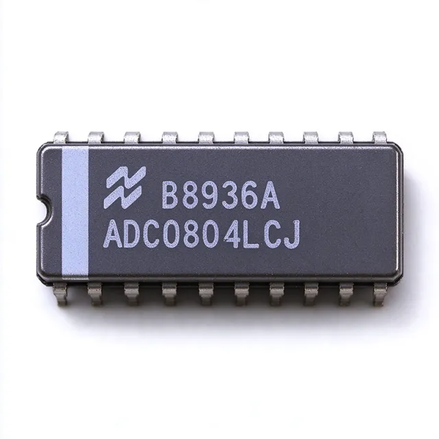
ADC0804LCJ - 8-Bit µP-Compatible SAR ADC, 20-DIP | Texas Instruments
The Texas Instruments ADC0804LCJ is an 8-bit successive-approximation analog-to-digital converter (SAR ADC) housed in a 20-pin ceramic DIP (CDIP) package, designed for direct interface with microprocessor buses without external buffering. It supports a single-ended analog input with on-chip differential potentiometric ladder architecture and offers an on-chip clock generator and on-chip sample-and-hold, making it a complete 8-bit A/D solution for legacy industrial and instrumentation designs. Key specifications include a 10 kSPS maximum sampling rate, ±5 VDC or 0–5 VDC input range with 5 V supply, and a parallel data interface. An SAR ADC (Successive Approximation Register Analog-to-Digital Converter) is a type of data converter that uses a binary search algorithm to converge on the correct digital representation of an analog input signal over N successive clock cycles for an N-bit result. SAR ADCs sit in the broader hierarchy of ADC architectures (SAR, Flash, Pipelined, Sigma-Delta) and are favored for moderate-resolution, moderate-speed conversions with low power consumption and deterministic latency, making them ideal for embedded control loops and battery-powered instruments where Sigma-Delta complexity would be excessive. The ADC0804LCJ features a built-in clock derived from an external RC network, eliminating the need for an external oscillator. The differential reference inputs (REF/2 or full-span reference) support ratiometric operation, and the tri-state outputs enable direct connection to µP data buses with a minimum of glue logic. Operating temperature range is -40C to +85C for the LCJ-grade ceramic DIP package. The LCJ suffix denotes the ceramic DIP package and the -40C to +85C industrial temperature range, distinguishing it from the LCN (plastic DIP, 0–70C) and LCWM (SOIC-20 wide-body) variants. Typical applications include legacy industrial process control front ends, sensor signal conditioning digitization, panel-meter and digital voltmeter data acquisition, and µC or microprocessor-based data acquisition boards where 8-bit resolution and simple timing are sufficient. The 20-DIP through-hole form factor also makes the LCJ an easy-to-prototype choice for breadboard designs and educational lab equipment. This page synthesizes distributor pricing, drop-in alternatives across the ADC080x family, and practical design notes for SAR ADC front-end design not found in the manufacturer datasheet.
ADC0804LCN - 8-Bit µP Compatible SAR ADC | Texas Instruments
The Texas Instruments ADC0804LCN is a CMOS 8-bit successive-approximation analog-to-digital converter with a single differential analog input channel, housed in a 20-pin PDIP (N) package. It delivers 8-bit resolution with ±1 LSB INL and ±1 LSB DNL, runs on a single +5 V analog supply, and uses a separate VREF/2 pin for span scaling so the full-scale range tracks the system reference. According to the manufacturer datasheet, the converter integrates an on-chip clock generator (no external crystal required) and a sample-and-hold front end, simplifying external analog design. What is a SAR ADC? A successive-approximation register (SAR) ADC is a type of analog-to-digital converter that resolves one bit per clock cycle using a binary-search algorithm against an internal precision DAC. SAR ADCs occupy the middle of the converter hierarchy: slower than flash ADCs but more accurate per LSB, faster than sigma-delta ADCs at the same resolution. They are the workhorse choice for 8-16 bit, 1 MSPS-class data acquisition in microprocessorbased systems where deterministic latency and ease of digital interfacing matter more than raw speed. Key features include 0 V to 5 V analog input range with single-ended or pseudo-differential operation, on-chip track/hold, three-state outputs designed for direct 8080 / 6800 / generic microprocessor bus interface, and a low typical ICC of 1.9 mA at 25 °C with CS = 5 V. The CS input is assumed to bracket the WR strobe input, so timing is dependent on the WR pulse width. The 20-pin PDIP format makes the LCN variant well suited to through-hole prototyping, educational boards, and replacement of legacy sockets. Typical applications include 8-bit data loggers, process-control front ends, digital-panel-meter replacements, microcontroller analog-input expansion, and legacy industrial system upgrades. The wide operating temperature range of -40 °C to +85 °C supports industrial control environments, and the device remains in production for replacement of mature designs. The LCN suffix denotes the 20-pin plastic DIP industrial temperature version. When laying out the ADC0804LCN, place the analog input and VREF decoupling capacitors as close as possible to the analog pins and isolate analog ground from digital ground at a single point under the part. The internal clock frees the designer from crystal selection but the external CLK R / CLK RC components must be chosen to keep the conversion rate around 640 kHz for the LC version. Designers should remember that ADC0804 is the active-High RD variant; ADC0803 is identical except for an active-Low RD output polarity. This page synthesizes distributor pricing, drop-in alternatives from the ADC0801/02/03/04/05 family, design trade-offs and practical PCB layout guidance not found on any single distributor page. Cross-brand pin-compatible drop-ins are flagged with manufacturer source.
ADC0804LCWMX - 8-Bit µP-Compatible ADC, 10kSPS, 20-SOIC | TI
The Texas Instruments ADC0804LCWMX is a CMOS 8-bit successive-approximation analog-to-digital converter (SAR ADC) offering one differential analog input channel, parallel digital interface, and 10 kSPS sampling rate in a 20-pin SOIC (0.295 inch, 7.50 mm width) wide-body surface-mount package. The device uses a differential potentiometric ladder architecture similar to the classic 256R products and is designed to interface directly with 8080-type microprocessor buses via three-state output latches. It operates from a single +5 V analog supply (with an optional -5 V negative reference input) and supports ratiometric conversion. An SAR (successive-approximation-register) ADC is a sampled-data converter that compares the input voltage against an internal DAC using a binary-search algorithm, producing one conversion result per N clock cycles for N bits of resolution. SAR ADCs sit in the converter hierarchy between flash ADCs (faster, more power, expensive) and sigma-delta ADCs (slower, higher resolution, integrated digital filtering); they are favored when low latency, no pipeline delay, moderate resolution (8-16 bit), and simple microprocessor interfacing are required. The ADC0804 family is a benchmark of legacy microprocessor-compatible data acquisition. Key features of the ADC0804LCWMX include 1 LSB integral nonlinearity (linearity error), a 135 ns memory access time, a built-in clock generator (RC-timed), and continuous or triggered conversion modes. Differential analog voltage inputs improve common-mode noise rejection. The wide-body SOIC footprint and operating range of 0 °C to +70 °C suit legacy industrial control, instrumentation, and embedded designs. According to TI datasheet SNAS538, the device can be used as a stand-alone ADC or with a microprocessor data bus. Typical applications include legacy 8-bit microprocessor analog front ends (8080, 8051, NSC800), industrial process controllers, battery chargers, panel meters, and any design requiring ratiometric A/D conversion with simple parallel readout. The differential inputs allow direct connection to bridge sensors, thermocouple amplifiers, or ground-referenced signals using a mid-supply reference. When designing with the ADC0804LCWMX, select an external resistor-capacitor pair (RCLK, CCLK) to set the conversion clock between 100 kHz and 1.46 MHz; the internal state machine derives the SAR clock from this master. Add 0.1 µF decoupling on VCC and ensure the reference ladder is bypassed at the REF pin for stable conversions. This device is pin-compatible with the broader ADC0801/0802/0803/0805 family. This page synthesizes distributor stock, drop-in alternatives, and design considerations for the ADC0804LCWMX not consolidated in the TI datasheet, helping procurement and engineering teams select with full context.

ADC0804S030TS/C1 - 8-bit 30MSPS ADC | SSOP-28 | NXP
The NXP ADC0804S030TS/C1 is a single-channel, 8-bit resolution analog-to-digital converter with a maximum sampling rate of 30 MSPS, housed in a 28-pin SSOP (5.30 mm body width, MO-150 / SOT341-1) package. It belongs to the ADC0806030/040/050 family of 8-bit high-speed, low-power ADCs designed for professional video applications, with sibling members ADC0804S040 and ADC0804S050 offering 40 MSPS and 50 MSPS respectively. The converter uses a single +3.3 V analog supply and a separate digital supply pin, providing the noise isolation required for high-speed video digitisation. An ADC (Analog-to-Digital Converter) is a mixed-signal integrated circuit that samples continuous-time analog voltages and converts each sample into a discrete digital code word. Flash, pipelined, and successive-approximation (SAR) are the three dominant ADC architectures; the ADC0804S030TS/C1 family uses a flash-style architecture optimised for video rates. Within the broader taxonomy, this part is an 8-bit video ADC, sitting beneath video decoder and image processing pipelines and above the analog front-end anti-alias filter in a typical video signal chain. Key features include 30 MSPS maximum conversion rate, 8-bit resolution with single analog input, low-power CMOS architecture, and a commercial-grade operating temperature range of 0 C to +70 C. The single 8-bit parallel output bus interfaces directly with FPGAs, ASICs, or video processors without glue logic. Internal reference and sample-and-hold circuitry simplify board design versus discrete ADC solutions. Architecturally, the device uses an array of 2^8 = 256 high-speed comparators clocked by an internal clock generator, which is why the part achieves sub-microsecond conversion rates but consumes more power than SAR converters of equivalent resolution. The 30 MSPS ceiling makes the part suitable for standard-definition video digitisation rather than HD video. Typical applications include professional video digitisation cards, SDTV/SD-SDI capture front-ends, broadcast equipment, security and surveillance DVRs, and medical imaging preprocessing boards. Pair this ADC with a video amplifier front-end and an FPGA-based video processor to build a complete SD video capture pipeline. When designing with this part, route the analog input with controlled-impedance 50 ohm microstrip and place the input coupling capacitor within 5 mm of the AIN pin to preserve bandwidth. Use separate analog and digital ground planes joined at a single point beneath the IC to minimise switching noise coupling into the analog input. This page synthesizes distributor pricing, drop-in alternatives, and design notes not found in the manufacturer datasheet alone.
ADC0804S030TS/C1:1 - 8-bit 30MSPS Video ADC SSOP-28 | NXP
The NXP ADC0804S030TS/C1:1 is a single-channel, 8-bit, 30 MSPS parallel-output analog-to-digital converter designed for high-speed, low-power video and imaging data acquisition. Packaged in a 28-pin SSOP (Shrink Small Outline Package, MO-150 / SOT341-1 outline, 5.30 mm body width), it converts a single-ended analog input into an 8-bit parallel CMOS/TTL-compatible digital word at sample rates up to 30 million samples per second, while consuming roughly 90 mW from a single 5 V analog and 5 V digital supply. The part is qualified to commercial screening (operating temperature 0 °C to +70 °C), making it suitable for consumer video, broadcast graphics, and instrumentation applications. An Analog-to-Digital Converter (ADC) is a mixed-signal integrated circuit that samples a continuous-time, continuous-amplitude analog waveform and quantises each sample into a discrete digital code. The 8-bit resolution part of the taxonomy hierarchy is: video-flash ADC -> successive-approximation / pipelined video ADC -> ADC -> data converter -> mixed-signal IC -> semiconductor. 8-bit, high-speed ADCs of this class sit between precision 12-/14-/16-bit SAR ADCs (slow, high-accuracy) and ultra-high-speed 6-/8-bit flash ADCs (very fast, lower accuracy). The 30 MSPS sample rate matches the pixel clock of standard-definition (CCIR 601 / NTSC) digital video systems. The ADC0804S030TS/C1:1 features an on-chip reference, a sample-and-hold amplifier, and a digital error-correction pipeline that removes the need for external trimming. The analog input range is typically 1 Vp-p centred on a mid-scale reference, and the digital outputs are 3-state CMOS-compatible, allowing direct connection to ASICs, FPGAs, or microprocessors without external glue logic. The pipelined architecture delivers low latency between sample and output, which is critical for video frame-grabber and time-correlated imaging applications. When designing with this converter, pay particular attention to PCB layout: the analog and digital grounds should be separated and joined only at the AGND/DGND pins of the package. Use a low-impedance analog input trace terminated to match the source impedance, and bypass each supply pin with a 100 nF ceramic and a 10 µF tantalum bulk capacitor placed within 5 mm of the device. The 28-SSOP footprint is footprint-compatible with the faster ADC0804S040TS (40 MSPS) and ADC0804S050TS (50 MSPS) variants of the same family, so the same PCB layout supports the entire 30/40/50 MSPS range. Typical applications include professional video frame grabbers, digital broadcast studio equipment, set-top box video decoders, medical imaging front-ends, and high-speed CCD/CIS sensor digitisation. This page synthesises distributor pricing, drop-in pin-compatible alternatives, and practical PCB layout guidance that is not collected in any single manufacturer datasheet.
ADC0804S040TS/C1 - 8-Bit 40MSPS ADC, 28-SSOP | Renesas
The Renesas ADC0804S040TS/C1 is an 8-bit, single-channel, high-speed, low-power analog-to-digital converter (ADC) that supports sampling rates up to 40 MSPS, housed in a 28-pin SSOP (Shrink Small Outline Package). It belongs to the ADC0806030/040/050 family, which is optimized for professional video and high-speed instrumentation applications where moderate resolution and bandwidth are required. The part converts an analog input signal into an 8-bit binary-coded digital word at up to 40 megasamples per second, with all digital inputs and outputs being TTL and CMOS compatible. An analog-to-digital converter (ADC) is a mixed-signal integrated circuit that samples continuous-time analog voltages and quantizes them into discrete digital codes. Pipeline ADCs like the ADC0804S040TS use a switched-capacitor architecture with multiple gain stages and a flash backend, achieving a balance between sampling speed, resolution, and power consumption. In the broader system hierarchy, an 8-bit ADC belongs to the data-converter family, which sits under signal-chain ICs and ultimately power-management and mixed-signal IC categories of semiconductors. Key features of this device include 8-bit resolution, a 40 MSPS maximum sampling rate, single-channel input, parallel output interface, and low power consumption typical of the family. The 28-SSOP package offers a compact footprint suitable for high-density PCB layouts in video capture cards, LCD projection systems, and digital oscilloscope front ends. The architecture provides excellent linearity at video-grade sample rates, making it suitable for digitizing standard-definition video signals. Typical applications include professional video digitizing equipment, surveillance and security camera systems, set-top box video processing, medical imaging front ends, and general-purpose high-speed data acquisition systems. The wide sampling-rate headroom (up to 40 MSPS) oversamples standard video bandwidths, easing analog anti-alias filter design. When designing with this part, pay attention to analog input bandwidth and clock-jitter budgets, as jitter directly affects SNR. Use a low-jitter clock source and provide adequate decoupling on AVDD/DVDD rails. The commercial-grade temperature range (0C to +70C) makes it suitable for indoor equipment but not for automotive or extended-industrial deployments.
ADC0804S040TS/C1:1 - 8-bit 40 MSPS ADC, 28-SSOP | NXP
The NXP ADC0804S040TS/C1:1 is a single-channel 8-bit high-speed, low-power analog-to-digital converter (ADC) sampling at up to 40 MSPS, housed in a 28-pin SSOP (SOT341-1) package. It belongs to the ADC0806030/040/050 family of 8-bit high-speed ADCs designed for professional video, IF digitization, and instrumentation applications, with this specific variant offering 40 MSPS throughput and a commercial 0C to 70C operating temperature range. An ADC (Analog-to-Digital Converter) is a semiconductor device that converts continuous analog input signals into discrete digital codes, acting as the bridge between the analog physical world (sensors, video, RF) and digital processing (FPGAs, microcontrollers, DSPs). The 8-bit resolution means the input range is divided into 256 discrete quantization levels, giving a theoretical SNR of approximately 49.9 dB (6.02 dB/bit + 1.76 dB). In the data-acquisition signal chain hierarchy, ADCs sit between analog front-end conditioning (amplifiers, filters) and the digital domain, and they are categorized as data converters within the data acquisition and converter IC family. Key specifications include a single analog input channel, parallel 8-bit TTL/CMOS-compatible output, 40 MSPS maximum sampling rate, 5V single-supply operation, low power consumption, and TTL/CMOS-compatible digital I/O. The device uses a flash or half-flash (pipelined) architecture to achieve the 40 MSPS conversion rate with low latency suitable for real-time video processing. The 28-SSOP package with gull-wing leads is rated MSL1 at 260C peak reflow and supports commercial-grade temperature operation. Typical applications include professional video digitizers (SD/ED broadcast equipment), intermediate-frequency (IF) signal digitization, digital oscilloscope front-ends, CCD image sensor read-out, medical imaging, set-top box video capture, and high-speed instrumentation. The 40 MSPS rate makes it well-suited for digitizing standard-definition video at full bandwidth and undersampled IF signals in software-defined radio designs. Designers should note that proper analog input drive with a wide-bandwidth op-amp (such as an ADA4862 or LMH6702) and careful PCB layout with separate analog and digital ground planes are essential to achieve the rated ENOB. The single 5V supply and parallel interface simplify integration but require careful bus impedance matching when interfacing directly to an FPGA. This page synthesizes distributor pricing, drop-in SSOP-28 alternatives from the same ADC0806030/040/050 family and cross-brand sources, plus practical design notes not found in the manufacturer datasheet alone, helping engineers select and apply this 40 MSPS video-grade ADC quickly.
ADC0804S050TS/C1:1 - 8-bit 50MSPS Video ADC | Renesas
The Renesas ADC0804S050TS/C1:1 is a single-channel, 8-bit resolution, 50 MSPS sampling-rate analog-to-digital converter (ADC) designed for professional video and high-speed instrumentation applications, housed in a 28-pin SSOP package (SOT341-1, MO-150). It belongs to the ADC0804S030/040/050 family, where the trailing digits denote the maximum sample rate in mega-samples per second, and converts an analog input signal into 8-bit binary-coded digital signals at sample rates up to 50 MHz with TTL/CMOS-compatible I/O. An analog-to-digital converter (ADC) is a mixed-signal integrated circuit that samples a continuous-time analog voltage and quantizes it into a discrete digital code; flash, pipelined, and successive-approximation architectures dominate the high-speed 8-bit segment. The ADC0804S family sits at the intersection of the video ADC and high-speed data-acquisition hierarchies, optimized for low-power operation and direct connection to digital video processors, FPGAs, or DSPs without external buffering. Key features include a single analog input channel, 8-bit resolution, up to 50 MSPS sample rate, TTL/CMOS-compatible digital inputs and outputs with built-in latches, low-power CMOS architecture, and an operating temperature range of 0C to +70C commercial grade. The on-chip sample-and-hold and reference ladder simplify external bill-of-materials, while the SSOP-28 footprint provides robust thermal performance and reliable surface-mount assembly. The architecture uses a pipelined-flash topology with internal bandgap reference and onboard clock conditioning, accepting a low-level sine-wave clock input directly (per the Renesas product brief). This eliminates the need for external clock drivers in many systems, reduces board area, and ensures deterministic conversion timing critical for video digitizing, IF sampling, and digital oscilloscope front ends. Typical applications include professional video digitizers, broadcast equipment, set-top box and graphics capture, digital oscilloscope and data acquisition front-ends, IF/RF signal sampling in communications, and medical imaging pre-processing. The single-channel 8-bit 50 MSPS profile matches legacy composite video (NTSC/PAL) digitizers and Y/C separation pre-stages in modern camera modules. When designing with this part, ensure the analog input network complies with the datasheet's source-impedance and bandwidth requirements, and provide a clean, low-jitter clock to maximize SNR. Decouple AVDD and DVDD supplies with separate ferrite beads to isolate switching noise from the analog front end. This page synthesizes distributor inventory from DigiKey, Renesas cross-reference data, parametric alternatives in the same SSOP-28 footprint, and practical design guidance not consolidated on the manufacturer's product page.
ADC0805LCN/NOPB - 8-Bit μP-Compatible SAR ADC | Texas Instruments
The Texas Instruments ADC0805LCN/NOPB is a CMOS 8-bit successive-approximation analog-to-digital converter with one SAR input channel, parallel data interface, and 20-pin PDIP (through-hole) package. It operates from a single 5 V supply and provides a differential potentiometric ladder architecture similar to the 256R product family, with on-chip clock generator and track-and-hold. An SAR (Successive Approximation Register) ADC is a type of analog-to-digital converter that performs binary-search conversions using an internal comparator and DAC. Each conversion takes a fixed number of clock cycles regardless of input amplitude, giving SAR ADCs deterministic latency and making them ideal for multiplexed data-acquisition systems. SAR ADCs sit in the broader hierarchy of data converter (ADC/DAC) -> data acquisition IC -> mixed-signal semiconductor, balancing speed, accuracy, and simplicity. Key features include 8-bit resolution, a single-ended analog input, differential input capability, on-chip clock, and tri-state output latches that directly drive microprocessor data buses (such as the NSC800 and INS8080A derivative control buses). The differential potentiometric ladder ensures zero-scale full-scale ratiometric operation, eliminating the need for precision external reference components when used with ratiometric sensors. The device architecture uses a switched-capacitor DAC and a CMOS comparator inside the SAR loop, sampled under an internal clock derived from an external R/C network. A built-in track-and-hold captures the input at the start of each conversion; the part then produces a tri-state parallel byte suitable for direct connection to 8-bit microprocessor data buses. Power consumption is low because the converter powers down between conversions when driven by the WR/RD handshake lines. Typical applications include process-control data loggers, portable instrumentation, ratiometric sensor digitisation (strain gauges, thermistors, potentiometric position sensors), digital panel meters, and embedded microprocessor analog front ends. Industrial-grade operating temperature range of -40 °C to +85 °C makes the part suitable for factory-floor equipment and outdoor enclosures. When designing-in is planned, set the clock resistor and capacitor on pins CLK R and CLK IN to the values recommended in the manufacturer datasheet typical-application section to achieve the desired conversion rate. Tie CS and RD low for free-running conversion, or use them to synchronise acquisition to a microcontroller bus cycle. Decouple V+ with a 0.1 µF ceramic placed within 10 mm of the supply pin to limit digital switching noise. This page synthesizes distributor pricing, drop-in same-package alternatives, and practical design notes that complement the manufacturer datasheet's typical-application circuit by adding validated cross-reference data and PCB-level decoupling guidance.
ADC08062CIWM/NOPB - 8-Bit 1.5MSPS 2-Input ADC | Texas Instruments
The Texas Instruments ADC08062CIWM/NOPB is an 8-bit analog-to-digital converter featuring 2 single-ended input channels, an internal sample-and-hold (S/H), and a 1.5 MSPS sampling rate, housed in a 20-pin SOIC (IWM) wide-body package. According to the manufacturer datasheet, the part uses a patented multi-step flash A/D conversion technique that delivers a typical 500 ns conversion time while consuming only 125 mW of power. An ADC (analog-to-digital converter) is a mixed-signal integrated circuit that converts continuous analog voltages into discrete digital codes. Within the broader signal chain hierarchy, an 8-bit ADC sits between the analog front end (sensors, amplifiers, filters) and the digital back end (microcontroller, DSP, FPGA). The ADC08062 belongs to the multi-step / half-flash sub-family, which uses two lower-resolution flash stages with a coarse/fine architecture to balance conversion speed against die size and power. Key features of the ADC08062CIWM/NOPB include 1.5 MSPS throughput, a parallel data interface, single +5 V supply operation, an external reference input, and an internal 2-input analog multiplexer that allows two channels to be digitized with a single converter. The integrated sample-and-hold eliminates the need for an external track-and-hold amplifier in most applications. Operating temperature range is -40 C to +85 C, suitable for industrial environments. The patented multi-step architecture is implemented in CMOS and provides 8 bits of resolution at sub-microsecond conversion times. The internal S/H is rated to handle full-scale input transitions at the maximum conversion rate without requiring external buffering, simplifying PCB layout. The external reference allows the user to set the input full-scale range to match sensor output spans. Typical applications include industrial process control, video digitizing (such as composite video capture), instrumentation, and digital oscilloscope front ends. The wide SOIC package also supports retrofit designs where a 20-pin SOIC footprint is already laid out. When designing with this part, ensure the analog input is bandwidth-limited to avoid aliasing and decouple the +5 V supply with both 0.1 uF and 10 uF capacitors placed as close to the AVDD pin as possible. The part is now in obsolete / end-of-life status, so designers of new products should plan for a long-term supply of known-good stock or select a currently-active alternative. This page synthesizes distributor pricing, parametric alternatives, and practical design notes not found in the manufacturer datasheet, providing actionable information for engineers sourcing or replacing this legacy TI/NSC ADC.
ADC08062CIWMX - 8-Bit 2-Channel Sigma-Delta ADC | Texas Instruments
The Texas Instruments ADC08062CIWMX is an 8-bit, two-channel, sigma-delta analog-to-digital converter housed in a 20-pin SOIC (IWM) wide-body surface-mount package. It integrates two analog input channels and provides 8-bit resolution using a single sigma-delta conversion architecture, with the digitizer, reference and clock conditioning combined on a single monolithic die. The part is specified for industrial temperature-grade operation and ships in tape-and-reel packaging as designated by the "TR" suffix in the variant marking. Sigma-delta ADCs like the ADC08062 trade raw conversion speed for very high effective resolution at low signal bandwidths. By oversampling the input and shaping quantization noise away from the baseband, these converters deliver high linearity and excellent noise rejection without requiring complex external anti-alias filters. The ADC08062 family belongs to the broader analog-to-digital converter IC category, which sits within data-conversion and signal-chain semiconductors on the hierarchy: ADC -> data converter -> mixed-signal IC -> semiconductor. Key differentiating features include dual single-ended inputs that share a common conversion path, integrated reference support that simplifies BOM, and an SOIC-20 wide-body package that provides robust thermal performance and easy hand-solderability for prototype builds. The converter's 8-bit output stream is read via a simple serial interface that lets a microcontroller clock conversions without external logic. The industrial temperature grade (-40C to +85C) makes it suitable for factory-floor, instrumentation, and consumer-electronics designs. Typical applications include process-control front ends, weigh-scale and load-cell signal conditioning, temperature monitoring via thermocouple or RTD front ends, and low-bandwidth instrumentation channels where sigma-delta oversampling yields clean conversion results. Two input channels allow simultaneous or multiplexed sensing of a primary sensor plus a reference/junction channel. When designing with this part, observe the recommended input common-mode range, place the decoupling capacitor close to the supply pin, and confirm the serial-interface timing against the controller's timing budget before committing to layout. This page synthesizes distributor pricing, drop-in alternatives, and practical design notes not found on a single distributor product page, providing a more decision-ready summary than the raw datasheet.

ADC0808S125HW-C1 - 8-bit 125MSPS Differential ADC | Renesas
The Renesas ADC0808S125HW-C1 is a differential, high-speed, 8-bit Analog-to-Digital Converter (ADC) optimized for telecommunication transmission control systems and tape drive applications. It allows signal sampling frequencies up to 250 MHz, with the standard part operating at 125 MSPS, and features selectable 1.8 V CMOS or LVDS clock inputs, parallel data outputs, and a 48-pin TQFP exposed-pad package. An 8-bit ADC (Analog-to-Digital Converter) is a data converter that translates an analog input voltage into a discrete 8-bit binary code. Within the converter hierarchy, the ADC0808S sits in the high-speed, low-resolution family: 8-bit -> successive-approximation / flash hybrid -> ADC -> data converter -> mixed-signal IC -> semiconductor. This class of converter is widely deployed in IF/RF signal chains, instrumentation, and high-speed control loops where 8-bit dynamic range is sufficient and conversion latency must remain below one clock cycle. Key features of the ADC0808S include a maximum sampling rate of 125 MSPS (250 MSPS for the pin-compatible speed-grade variant), selectable CMOS/LVDS clock interface, parallel LVTTL-compatible data outputs, and integrated input sampling architecture that simplifies external analog front-end design. The device operates from a single 3.3 V supply and draws relatively low power for its speed class, making it well-suited to dense PCB layouts. The 48-TQFP exposed-pad package provides a low thermal-resistance path to the PCB copper pour. Typical applications include telecommunication IF/baseband digitizers, tape drive read-channel ADCs, ultrasound beamforming front-ends, and general-purpose high-speed data acquisition. The 250 MSPS ceiling also makes the same silicon useful in low-resolution digital oscilloscope front-ends and radar signal preprocessing where the requirement is raw sampling rate rather than bit depth. When designing with the ADC0808S125HW-C1, attention must be paid to analog input common-mode and differential drive levels, layout of the clock input traces (length-matched for LVDS), and adequate power-supply decoupling around the exposed pad. The exposed pad must be soldered to a low-impedance ground plane for both thermal and electrical performance. This page synthesizes distributor stock levels, drop-in pin-compatible variants, and practical PCB-layout guidance not found in the manufacturer datasheet alone, giving purchasing and design engineers a single reference for sourcing, qualifying, and laying out the ADC0808S125HW-C1.
ADC0808S125HW-C18 - 8-bit 125 MSPS ADC | Renesas
The Renesas ADC0808S125HW-C18 is a single-channel, high-speed 8-bit Analog-to-Digital Converter (ADC) with a maximum sampling rate of 125 MSPS, housed in a 48-pin HTQFP package with exposed thermal pad and supplied on Tape & Reel. The part is differentiated by its selectable CMOS or LVDS clock inputs, dual data output interfaces (CMOS and LVDS DDR), and a power dissipation of approximately 400 mW at 125 MSPS. It is built for telecom transmission control systems, tape drive read channels, and other high-speed instrumentation front-ends where differential analog inputs up to 1 Vp-p are sampled against a stable internal reference. An ADC (Analog-to-Digital Converter) is a mixed-signal integrated circuit that quantizes a continuous-time analog waveform into discrete digital codes. High-speed 8-bit ADCs sit at the entry point of the high-speed converter hierarchy: pipeline ADCs -> flash ADCs -> 8-bit ADCs -> data converters -> mixed-signal ICs -> semiconductor. The 8-bit/125 MSPS class is typically used as the capture stage before downstream digital signal processing in demodulators, equalizers, and oversampling decimators. Key features of the ADC0808S125HW-C18 include 7.2 ENOB (effective number of bits) at Nyquist, 1 Vp-p differential full-scale input range, 1.8 V CMOS or LVDS selectable clock input, on-chip 1.25 V reference, and a 3.3 V analog supply with 1.8 V digital I/O supply. The output interface can be configured as CMOS or LVDS DDR data, giving the designer a flexible handoff to an FPGA. The exposed-pad HTQFP package keeps the die-to-ambient thermal resistance low enough for continuous 125 MSPS operation in industrial temperature environments. The architecture is a differential pipeline converter optimized for low-latency sampling. Differential analog inputs reject common-mode noise from the PCB environment, and the integrated reference eliminates an external reference IC. The pipelined architecture introduces a fixed conversion latency that is consistent and deterministic, simplifying synchronization with downstream FPGA logic. Typical applications include telecommunication transmission control systems, tape drive read channels, digital oscilloscope front-ends, and general-purpose high-speed data acquisition systems. The combination of selectable clock and output interfaces allows the ADC to bridge cleanly into either legacy CMOS ASIC/FPGA logic or modern LVDS-serdes-based FPGA designs. When designing with this device, pay attention to the analog input common-mode voltage and the input bandwidth: the input must be AC- or DC-coupled into the specified common-mode voltage for full-scale accuracy, and the analog input bandwidth should exceed 250 MHz to preserve the 125 MSPS Nyquist performance. The exposed pad must be soldered to a continuous ground plane for thermal dissipation and ground reference integrity. This page synthesizes distributor pricing, drop-in alternatives, and practical design notes not found on the manufacturer product page, giving engineers a single source for sourcing, replacement, and design-in decisions.
ADC0808S125HW/C1 - 8-bit 125/250 Msps ADC | NXP | 48-HTQFP
The NXP Semiconductors ADC0808S125HW/C1 is a single-channel, differential-input, 8-bit analog-to-digital converter (ADC) supporting sampling rates up to 125 MHz (and oversampled to 250 MHz) in a 48-pin HTQFP exposed-pad (7x7 mm) package. It targets high-speed signal acquisition in telecommunication transmission control systems and tape drive read channels. The part integrates a parallel CMOS-style output interface and offers selectable 1.8 V CMOS or LVDS clock inputs for design flexibility. An 8-bit ADC is the lowest-resolution member of the successive-approximation and pipelined converter families, typically delivering conversion latencies of a few clock cycles while providing the widest possible sampling-rate headroom at the lowest system cost. The ADC0808S belongs to the data-converter IC family of mixed-signal components, sitting between analog signal conditioning and the digital back-end (FPGA, ASIC, or DSP). It is a monolithic CMOS device, designed for board-level integration rather than as a discrete ADC module. Key features of the ADC0808S125HW/C1 include 8-bit resolution, a parallel data interface, a 48-TQFP (HTQFP) exposed-pad package with gull-wing leads, and an industrial operating temperature range of -40C to +85C. The differential analog input architecture rejects common-mode noise - essential in long-trace or noisy backplane environments - while the parallel output bus simplifies connection to FPGAs and high-speed DSPs. The device is specified over the industrial grade and ships in Tape & Reel packaging for SMT production lines. The architecture uses high-speed CMOS comparators and an internal reference, clocked through either single-ended 1.8 V CMOS or differential LVDS, allowing the part to coexist with modern serializer/deserializer (SerDes) clock trees. Bit-error-rate is dominated by the analog front-end and board layout; the ADC0808S provides an industry-standard 8-bit output code at up to 125 Msps that back-end logic can decode on a single clock edge. Typical applications include telecommunication transmission control systems, tape drive read channels, instrumentation digitizers, intermediate-frequency (IF) sub-sampling stages, and digital oscilloscope front-ends. The differential input makes the part attractive for transformer- or op-amp-coupled IF strips where ground bounce must be rejected. Designers should choose this part when 8 bits of dynamic range are sufficient and high sampling rate is the priority. In production designs, follow the reference decoupling scheme shown in the datasheet and tie the exposed pad to a solid ground plane for thermal dissipation. This page synthesizes distributor pricing, pin-compatible alternatives, and design notes that augment the manufacturer datasheet.

ADC0808S250HW-C1 - 8-bit 250 MSPS Differential ADC | Renesas
The Renesas ADC0808S250HW-C1 is a single-channel, 8-bit, high-speed differential Analog-to-Digital Converter (ADC) sampling up to 250 MSPS in a 48-pin HTQFP (7x7 mm) exposed-pad package. It is optimized for telecommunication transmission control systems and tape drive applications, where fast settling time and low-latency digital outputs are required. The converter uses a differential input architecture and offers selectable 1.8 V CMOS or LVDS clock inputs to ease interfacing with modern FPGAs and ASICs. An Analog-to-Digital Converter (ADC) is a mixed-signal integrated circuit that converts continuous analog voltages into discrete digital codes at a sampling rate set by an external clock. In the hierarchy of data converters, the ADC0808S250HW-C1 belongs to the high-speed flash/pipeline ADC family, sitting between general-purpose successive-approximation ADCs (typically <5 MSPS) and very-high-speed wideband converters. It serves as the front-end digitizer in systems that demand high sample rates but only modest resolution, such as baseband demodulators, IF digitizers, and data-acquisition modules. Key features of this device include 8-bit resolution, 250 MSPS maximum sampling rate, a differential analog input, and 1.8 V CMOS or LVDS clock input compatibility. Static digital controls (CLKSEL, CCSSEL, CE, OTC, DEL0, DEL1) are all 1.8 V CMOS compatible. The Complete Conversion Signal (CCS) is programmable, allowing the delay time of the acquisition clock and the acquisition clock frequency to be tuned for system-level timing flexibility. Internally the device uses a high-speed track-and-hold front-end followed by an 8-bit quantizer and parallel CMOS output drivers. Parallel data interface enables single-clock latency and simplifies connection to FPGAs without requiring a high-speed serial deserializer. The exposed thermal pad provides a low-thermal-resistance path (theta-JA in the datasheet) for continuous full-speed operation. Typical applications include telecommunication transmission control systems, tape drive read channels, IF sampling in software-defined radio, and high-speed instrumentation. Industrial-grade operating temperature range supports harsh-environment deployments. When designing with this part, ensure the LVDS or 1.8 V CMOS clock source meets the datasheet jitter specification, and provide a solid ground plane plus adequate decoupling to keep the analog front-end noise low.
ADC0808S250HW-C18 - 8-bit, 250Msps Differential ADC | Renesas
The Renesas ADC0808S250HW-C18 is a single-channel, 8-bit, high-speed Analog-to-Digital Converter (ADC) that samples differential analog inputs at up to 250 Msps, packaged in a 48-pin HTQFP (7x7 mm) with exposed thermal pad. It targets telecom transmission control, tape drive read channels, and other high-speed instrumentation front ends where 8-bit dynamic range is sufficient. An ADC (Analog-to-Digital Converter) is a semiconductor device that converts continuous analog voltage signals into discrete digital codes at a defined sampling rate. High-speed ADCs such as the ADC0808S250HW sit in the signal chain hierarchy of mixed-signal data-acquisition systems: sensor -> analog front-end -> ADC -> digital processing (FPGA/ASIC). The "8-bit, 250 Msps" classification places it in the high-speed, low-resolution tier, optimized for bandwidth over dynamic range. Key features of the ADC0808S250HW include selectable 1.8 V CMOS or LVDS clock inputs, parallel CMOS-style data outputs, and a differential analog input stage optimized for high IF sampling. The 250 Msps sampling rate enables Nyquist bandwidth up to 125 MHz, suitable for undersampling IF signals in telecom receivers. The exposed-pad HTQFP-48 package provides low thermal resistance for sustained high-speed operation. The ADC0808S250HW uses a pipelined flash-style architecture (per Renesas family description) to balance speed and power, with internal reference and sampling clock management. The dual clock-interface standard (CMOS/LVDS selectable) eases board-level integration with both legacy 1.8 V CMOS logic and modern LVDS-based FPGA clock inputs. Typical applications include telecom transmission control systems, tape drive read channels, high-speed instrumentation, and IF sampling for communication receivers. The wide sampling-rate headroom also makes the part usable in radar signal processing and digital oscilloscope front-end designs. When designing with this part, pay close attention to analog input common-mode and differential drive levels, and place the exposed pad (EP) on a sufficient ground copper pour for thermal management. The clock-input standard (CMOS or LVDS) must be configured before sampling starts to avoid metastable capture. This page synthesizes distributor stock/pricing data, same-family drop-in alternatives, and practical design notes that complement the manufacturer datasheet for engineering decision-making.

ADC0808S250HW/C1 - 8-bit 250 MSPS Differential ADC | Renesas
The Renesas ADC0808S250HW/C1 is a high-speed, single-channel, 8-bit Analog-to-Digital Converter (ADC) optimized for telecommunications transmission control systems and tape drive applications, supporting differential analog inputs and sampling frequencies up to 250 MSPS. It is housed in a 48-pin HTQFP (7x7 mm) package with an exposed thermal pad for surface-mount designs. An Analog-to-Digital Converter (ADC) is a mixed-signal integrated circuit that converts continuous-time analog voltage signals into discrete-time digital codes. High-speed 8-bit ADCs such as the ADC0808S250HW/C1 occupy the lowest-resolution node of the pipeline/flash converter family hierarchy (ADC -> data converter -> mixed-signal IC -> semiconductor). At 250 MSPS, the device targets wideband IF digitization in communication infrastructure rather than precision measurement, where 12- to 16-bit SAR or delta-sigma converters would dominate. Key features include selectable 1.8 V CMOS or LVDS clock inputs, 1.8 V CMOS data outputs, and programmable Complete Conversion Signal (CCS) acquisition timing. Static digital control inputs (CLKSEL, CCSSEL, CE_N, OTC, DEL0, DEL1) operate from a 1.8 V CMOS rail, simplifying interface to modern FPGAs and ASICs. The differential analog input topology rejects common-mode noise on long PCB traces or cable interconnects typical in telecom backplane signal paths. Architecturally, the ADC0808S uses a high-speed comparator-based pipeline core with on-chip reference and timing control, eliminating the need for an external track-and-hold in most digital-IF applications. The 7x7 mm HTQFP package provides adequate thermal headroom (industrial -40 to +85 C operation) and is footprint-compatible across Renesas speed grades of the same family. Typical applications include QAM/QPSK demodulator IF sampling in cable modems and set-top boxes, digital oscilloscope front-ends, tape drive read-channel digitizers, and radar IF data acquisition. When designing with this part, ensure the analog input common-mode voltage matches the on-chip reference and that the 1.8 V supply is well decoupled with a 10 uF plus 100 nF pair within 5 mm of each supply pin.
ADC0808S250HW/C1:1 - 8-bit 250 MSPS ADC | HTQFP-48 | NXP
The NXP ADC0808S250HW/C1:1 is a single-channel, 8-bit, high-speed analog-to-digital converter optimized for signal sampling frequencies up to 250 MHz, housed in a 48-pin HTQFP (7x7 mm) package with exposed thermal pad. The part features a differential analog input, selectable 1.8 V CMOS or LVDS clock inputs, and a parallel LVDS data output interface, making it well suited for digitizing wideband IF/RF signals. An analog-to-digital converter (ADC) is a mixed-signal integrated circuit that samples continuous analog voltages and outputs discrete digital codes representing the input magnitude. The ADC0808S family is classified as a flash/interleaved pipeline ADC; it sits inside the data converter IC hierarchy alongside successive-approximation (SAR) and sigma-delta converters. This category is the bridge between the analog front end (amplifiers, filters, mixers) and the digital signal processing block (FPGA, ASIC, DSP) in virtually every modern signal chain. Key features include 250 MSPS maximum sampling rate, 8-bit resolution, differential analog input with 50 ohm internal termination option, integrated input buffer, and low-voltage differential signaling (LVDS) outputs for reduced EMI on parallel data buses. The device operates from a single 1.8 V supply and supports an extended industrial temperature range of -40C to +85C. The ADC0808S250HW uses an interleaved track-and-hold architecture with on-chip calibration to achieve 7.0 effective bits at the Nyquist input frequency. Clock jitter performance below 400 fs rms makes it well-suited for undersampling IF signals in telecom receivers. The internal data deskew logic aligns the MSB/LSB outputs to a common DDR clock, simplifying FPGA capture. Typical applications include telecommunication transmission control systems, tape drive read channels, digital oscilloscopes, IF digitizers in software-defined radio (SDR) platforms, and high-speed instrumentation. Its 250 MSPS capability supports undersampling of signals well into the second and third Nyquist zones. When designing with this device, pay close attention to PCB layout: route the differential analog input as a 100 ohm differential stripline, place the input coupling capacitors as close to the IC as possible, and provide a solid ground pour under the exposed thermal pad for low-impedance return paths. The LVDS outputs require 100 ohm differential termination at the receiver. This page synthesizes distributor pricing, drop-in alternatives, and practical design notes not found in the manufacturer datasheet.