EP4CE55F29C8L vs EP4CE55F29C7N Ikinahambing
Detalyadong pagkakahiwalay na pagkakahambing ng EP4CE55F29C8L sa pamamagitan ng Intel at EP4CE55F29C7N sa pamamagitan ng Intel. Ikinahambing ang mga pangunahing paglalarawan, mga tama ng elektriko, paakay, kalagayan ng buhay, presyo, at pagkakaroon upang makita ang pinakamahusay na komponente para sa iyong mga kinakailangang pang disenyo.

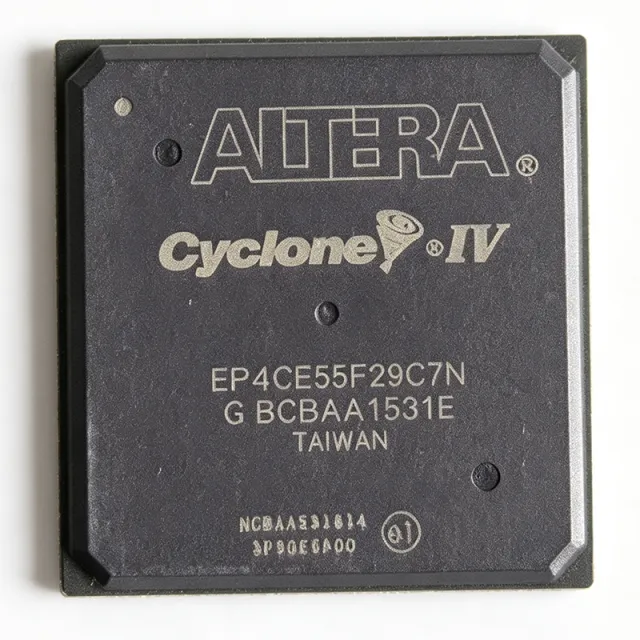
Pagsanggunian na paghahambing
| Parametro | EP4CE55F29C8L | EP4CE55F29C7N |
|---|---|---|
| Brand | Intel | Intel |
| Kategorya | FPGA & CPLD | FPGA & CPLD |
| Katayuan ng Lifecycle | Aktibo | Aktibo |
| Presyo ng Yunit (USD) | — | $138.00 |
| Family | Cyclone IV E | Cyclone IV E |
| Logic Elements | 55,856 | — |
| Embedded Memory Bits | 2,396,160 bits | — |
| Embedded Memory (M9K Blocks) | 260 blocks | — |
| Embedded 18x18 Multipliers | 156 | — |
| Maximum User I/O Pins | 374 | — |
| PLLs | 4 | — |
| Global Clock Networks | 20 | — |
| Core Voltage | 1.2 V | 1.2 V nominal |
| Process Technology | 60 nm (low-power) | — |
| Packhaging | 780-ball FBGA (F29), 29x29 mm, 1.0 mm pitch | 780-ball FBGA (F29) |
| Speed Grade | C8 (commercial, 8 speed bin) | -7 (C7) |
| Temperature na Operasyon | 0C to +85C (commercial, 'L' suffix) | 0C to +85C (commercial) |
| Uri ng Pagpapasok | Surface Mount (BGA) | Surface Mount |
| Tindminan RoHS | Compliant | Compliant (LEAD FREE) |
| Configuration Schemes | AS, PS, JTAG, FPP | — |
| JTAG (IEEE 1149.1) | Supported | — |
| Configuration Memory | SRAM-based (external flash required) | — |
| Logic Elements (LE) | — | 55,856 |
| Configurable Logic Blocks (CLBs) | — | 3,491 |
| Total RAM Bits | — | 2,396,160 |
| Embedded Multipliers (18x18) | — | [DATA_NEEDED: 18x18 multiplier count] |
| User I/O Count | — | 374 |
| Number of PLLs | — | [DATA_NEEDED: PLL count] |
| Package Dimensions | — | 29 mm x 29 mm |
| Ball Pitch | — | 1.0 mm |
| Volte ng Pagbibigay | — | 1.2 V |
| Lead Free | — | Yes |
| Configuration Mode | — | JTAG, Active Serial, Passive Parallel |