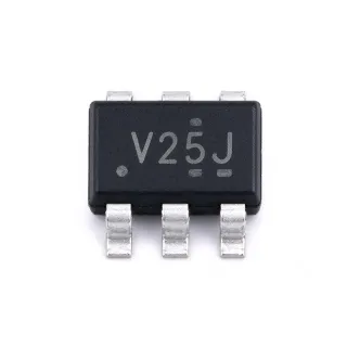
LM2904LVQDGKRQ1 - 5.5V 1MHz Automotive Dual Op Amp | Texas Instruments
MPN: LM2904LVQDGKRQ1 ✓ NakahandaLM2904LVQDGKRQ1 Ulas
An operational amplifier is an analog integrated circuit that uses high-gain differential amplification to compare an inverting input with a non-inverting input. Within the broader hierarchy, it is a voltage-feedback amplifier, an amplifier IC, and a signal-conditioning semiconductor. The dual configuration allows one device to process two related channels, reducing board area when both channels share the same supply and ground reference.
The LM2904LV-Q1 family targets automotive and industrial low-voltage applications where supply efficiency, cost, and dependable operation are important. The 2.7 V to 5.5 V operating range supports systems powered from regulated 3.3 V and 5 V rails. Its 1 MHz bandwidth makes it suitable for general-purpose amplification, buffering, voltage comparison, filtering, and sensor-interface functions rather than high-speed signal processing.
The dual amplifier architecture is useful in sensor conditioning, current sensing, control loops, line-driver buffers, and automotive body electronics. Each amplifier can be used independently, allowing the two channels to monitor complementary signals or perform separate functions in a compact circuit. Input and output stability, common-mode range, and output-drive capability should be checked against the actual signal levels and load conditions.
The principal design trade-off is that this is a general-purpose, low-voltage amplifier rather than a precision or high-speed device. Its 3 mV offset specification is appropriate for many sensing and control paths, but systems requiring tighter offset accuracy need to evaluate the bias current, input voltage range, noise, and application error budget.
This page combines the manufacturer specifications, package information, application guidance, comparison parameters, and practical drop-in selection notes for engineers evaluating the LM2904LVQDGKRQ1.
Mga alternatibo na pwedeng ilagay na LM2904LVQDGKRQ1 — parehas na package, pin-to-pin na katugmang. Hindi kasama ang mga bahagi ng iba't-ibang package na nangangailangan ng pagpapaayos ng PCB.
LM2904LVQDRQ1
✅ Drop-InMagkontak para sa presyo
Tingnan ang Datasheet →LM2904LVQDGKRQ1
✅ Drop-InMagkontak para sa presyo
Tingnan ang Datasheet →LM2904LVQDGKRQ1-Q1
✅ Drop-In ⚠️ Mga Talaan Hindi Naiwerikmo📋 Alternatibo na Reference (hindi sa katalogo)
LM2904QDGKRQ1
✅ Drop-In ⚠️ Mga Talaan Hindi Naiwerikmo📋 Alternatibo na Reference (hindi sa katalogo)
LM2902LVQDGKRQ1
✅ Drop-In ⚠️ Mga Talaan Hindi Naiwerikmo📋 Alternatibo na Reference (hindi sa katalogo)
LM2904LVQDGKRQ1 Mga Pinakamataas na Rating at Electrical Characteristics
| Product Type | Dual operational amplifier |
| Number of Amplifier Circuits | 2 circuits |
| Supply Voltage Range | 2.7 V to 5.5 V |
| Maximum Supply Voltage | 5.5 V |
| Gain-Bandwidth Product | 1 MHz |
| Input Offset Voltage | 3 mV |
| Automotive Qualification | AEC-Q100 automotive-grade device |
| Packhaging | 8-VSSOP |
| Uri ng Pagpapasok | Surface mount |
| Standard Product | General-purpose operational amplifier |
Gabay sa Pin Configuration ng LM2904LVQDGKRQ1 8-vssop
Pin configuration para sa LM2904LVQDGKRQ1 (8-vssop package). Ang analog component na ito ay may input, output, at power supply pins. Sumangguni sa datasheet ng manufacturer para sa offset null, compensation, at enable pin configurations. Perpekto para sa signal conditioning at amplifier circuits.

Wala ng detalyadong pinout data na magagamit para sa LM2904LVQDGKRQ1.
Sumangguni sa datasheet para sa buong pin configuration.
Tipikal na mga Gamit
LM2904LVQDGKRQ1 ay nararapat para sa 6 aplikasyons: Automotive Sensor Signal Conditioning, 3.3V Control-Loop Amplification, Automotive Actuator Drive Interface, Battery-Powered Monitoring Circuit, Active Filtering and Buffering, Low-Voltage Industrial Interface.
Automotive Sensor Signal Conditioning
The LM2904LVQDGKRQ1 fits low-voltage automotive sensor conditioning because it accepts a 2.7 V to 5.5 V supply and provides two amplifier channels for related inputs. Its 1 MHz gain-bandwidth product is adequate for buffering and modest-gain stages in 3.3 V or 5 V sensor interfaces. The 3 mV input offset specification must be included in the system error budget, while the dual layout helps reduce board area compared with two separate single amplifiers.
Inirekomenda
3.3V Control-Loop Amplification
In a 3.3 V control system, the LM2904LVQDGKRQ1 can amplify error signals, support active filtering, or buffer a feedback node. Its 2.7 V lower supply limit provides operating margin below a nominal 3.3 V rail, while the 1 MHz bandwidth supports general-purpose control-loop functions. The designer should verify the input common-mode range, output swing, stability with the selected feedback network, and the offset contribution of 3 mV.
Inirekomenda
Automotive Actuator Drive Interface
The dual amplifier can serve as the input and feedback stage for a low-voltage automotive actuator interface. Placing the device between a sensor or command signal and a downstream driver stage can improve drive capability and isolate the source from the load. The 5.5 V maximum supply keeps the device aligned with low-voltage automotive rails, while the 3 mV offset and 1 MHz bandwidth define the main error and dynamic-performance constraints.
Inirekomenda
Battery-Powered Monitoring Circuit
For a battery-powered monitor, the LM2904LVQDGKRQ1 can amplify a low-level sensor signal near a regulated 3.3 V rail. Its low-voltage supply operation reduces the need for a high-voltage amplifier in portable or energy-limited systems, and two channels can monitor two measurements with a shared supply. The application must account for battery variation, common-mode input limits, output headroom, and the offset error introduced by the 3 mV specification.
Inirekomenda
Active Filtering and Buffering
The LM2904LVQDGKRQ1 is suitable for first-order active filters, unity-gain buffers, and general analog conditioning when the required bandwidth is near the 1 MHz gain-bandwidth class. The dual package allows two filters or buffers to share one package and supply node. Design the feedback network around the actual load and source impedance, and confirm that the operating point keeps both input and output signals within the device's voltage limits.
Inirekomenda
Low-Voltage Industrial Interface
The LM2904LVQDGKRQ1 can support general-purpose industrial interfaces running from regulated 3.3 V or 5 V supplies. It can buffer transducer outputs, compare control signals, or provide gain before a communications or power-control stage. The automotive-qualified family status is useful when ruggedized sourcing is preferred, but the designer should still verify the exact temperature range, input/output limits, and board-level noise behavior.
Inirekomenda
Buod ng mga Inirekomendang Produkto
Impormasyon ng Talumpati sa Engineering for LM2904LVQDGKRQ1 — ikabit, gabay sa disenyo, at impormasyon ng pagsunod sa kautusan.
Paunawang Hanapin
Ikabit sa Mga Alternatibo
| Parametro | Ito ang Producto | LM2904LVQDRQ1 | LM2904LVQDGKRQ1 | LM2904LVQDGKRQ1-Q1 | LM2904QDGKRQ1 | LM2902LVQDGKRQ1 |
|---|---|---|---|---|---|---|
| Brand | Texas Instruments | Texas Instruments | Texas Instruments | Texas Instruments | Texas Instruments | Texas Instruments |
| Package | 8-VSSOP | 8-VSSOP | 8-VSSOP | 8-VSSOP | 8-VSSOP | 8-VSSOP |
| Amplifier Configuration | Dual, 2 circuits | Dual, 2 circuits | Dual, 2 circuits | Dual, 2 circuits | Dual, 2 circuits | Quad, 4 circuits |
| Automotive Grade | Yes | Yes | Yes | Yes | Yes | Yes |
Pangunahing mga Pagkakaiba
- Low-voltage operation (kumpara saLM2904QDGKRQ1)
- Dual-channel integration (kumpara saLM2902LVQDGKRQ1)
- Automotive-oriented family positioning (kumpara saLM2904LVQDRQ1)
Talaan ng Disenyo
Place the supply bypass capacitor as close as practical to the V+ and ground pins, and use a short, low-inductance return path. Keep input, feedback, and output routing compact because parasitic capacitance in the feedback network can alter stability. The exact decoupling value and layout should follow the manufacturer recommendations for the LM290xLV-Q1 family.
Do not assume that a 5.5 V maximum supply allows a 5.5 V signal at every pin. Check the input common-mode range and output swing before using the amplifier near either supply rail. For low-voltage designs, calculate the offset contribution from the 3 mV input-offset specification and confirm that the feedback network remains stable with the selected source and load impedances.
Estimated: the device power dissipation is approximately the supply voltage multiplied by total supply current plus output-stage load dissipation. The input values for an exact calculation are 5.5 V maximum supply and the application-specific supply current. Use the manufacturer thermal data and the actual board copper area for junction-temperature verification.
Impormasyon ng Pagsunod sa Kautusan
Texas Instruments identifies the LM2904LV-Q1 family as automotive-grade. Specific RoHS, REACH, lead-free, halogen-free, and conflict-minerals statuses require confirmation for the exact ordering code.