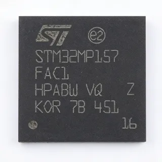
MPC8548EVTATGB - PowerQUICC III e500 MPU, 1.2 GHz | NXP
MPN: MPC8548EVTATGB ✓ NakahandaMPC8548EVTATGB Ulas
A PowerQUICC III processor is a system-on-chip (SoC) communications engine designed for networking, telecom, and embedded infrastructure equipment. Within the broader taxonomy, it sits at the intersection of microprocessor (MPU) and SoC platform - built on Power Architecture technology with on-chip peripherals that traditionally would require a separate chipset. This category targets high-throughput, deterministic packet and signal-plane processing rather than general-purpose compute.
Key features include 512 KB of internal SRAM, hardware-accelerated cryptography (AES, 3DES, SHA-1/MD5, Kasumi), RAIDEngine XOR acceleration for storage, and a 64-bit DDR1/DDR2 SDRAM memory controller with ECC support. The advanced interrupt controller and four 32-bit timers deliver deterministic real-time response for protocol stacks. Operating voltage domains at 1.0 V core and 1.8 V / 2.5 V / 3.3 V I/O simplify integration into 3.3 V-tolerant backplane designs.
The MPC8548EVTATGB engineering designation (suffix ATGB = 1.2 GHz, industrial temperature, lead-free FCBGA) places it in the higher-performing tier of the MPC8548 family. Pin-compatible variants like the MPC8547 and MPC8572 series share the same FCBGA-783 footprint with reduced or enriched peripheral mixes, enabling designers to migrate up or down without PCB rework. The device implements SMP- and AMP-capable coherency through its CoreNet-compatible interconnect on later derivatives.
Typical applications include multiservice routers, enterprise Layer 2/3 switches, wireless base stations, security appliances, RAID storage controllers, and industrial control planes. The combination of cryptographic acceleration, packet processing, and PCI Express host makes it well-suited for unified threat management (UTM) and IPSec-aware gateways where throughput per watt is critical.
When designing with this device, allocate ample PCB layers (typically 8-12) for FCBGA breakout, maintain DDR2 trace length matching within 25 mils, and sequence the 1.0 V core supply only after the 1.8 V auxiliary rail to avoid latch-up. A JTAG header compliant with IEEE 1149.1 is required for boundary-scan and code-load diagnostics. Watch thermal performance carefully - at 1.2 GHz the device dissipates approximately 8-12 W and benefits from airflow at the board edge.
This page synthesizes distributor pricing, parametric drop-in alternatives within the PowerQUICC III family, and PCB layout guidance beyond what is duplicated in the manufacturer datasheet summary.
Mga alternatibo na pwedeng ilagay na MPC8548EVTATGB — parehas na package, pin-to-pin na katugmang. Hindi kasama ang mga bahagi ng iba't-ibang package na nangangailangan ng pagpapaayos ng PCB.
Variante sa Seri na ito
Katulad na modelo sa serye na katugma sa pagpasok MPC8548EVTATGB (parehas na form factor at footprint) — pagkakaiba sa Core Architecture, RoHS Status, Maximum Core Frequency, Memory Controller, Operating Temperature.
MPC8547VTAQGB
✅ Drop-InMagkontak para sa presyo
Tingnan ang Datasheet →MPC8547EVTAUJB
✅ Drop-InMagkontak para sa presyo
Tingnan ang Datasheet →MPC8545VTAQGB
✅ Drop-InMagkontak para sa presyo
Tingnan ang Datasheet →MPC8548ECVTAQGB
✅ Drop-InMagkontak para sa presyo
Tingnan ang Datasheet →MPC8572ECVTAULE
✅ Drop-In📋 Alternatibo na Reference (hindi sa katalogo)
MPC8548EVTATGB Mga Pinakamataas na Rating at Electrical Characteristics
| Manufacturer | NXP Semiconductors (formerly Freescale) |
| Product Family | PowerQUICC III (MPC85xx) |
| Core Architecture | PowerPC e500 (32-bit superscalar) |
| Number of Cores | 1 |
| Maximum Core Frequency | 1.2 GHz |
| Packhaging | 783-FCBGA (29x29 mm) |
| Uri ng Pagpapasok | Surface Mount |
| Supply Voltage - Core | 1.0 V |
| Supply Voltage - I/O | 1.8 V / 2.5 V / 3.3 V |
| Temperature na Operasyon | -40C to +105C (industrial grade, AT suffix) |
| L1 Cache (per core) | 32 KB instruction + 32 KB data |
| On-chip SRAM | 512 KB |
| Memory Controller | DDR1/DDR2 SDRAM, 64-bit with ECC |
| Ethernet MAC | 4x 10/100/1000 Mbps (SGMII/RGMII/TBI) |
| High-speed Serial I/O | PCI Express x4, Serial RapidIO 1.2, 2x SGMII |
| Security Engine | AES, 3DES, SHA-1, MD5, Kasumi acceleration |
| RAID Acceleration | RAIDEngine XOR |
| Process Technology | 90 nm CMOS |
| Tindminan RoHS | Compliant (lead-free PB-free) |
| Lifecycle | Active - Not recommended for new designs at tail of family |
Gabay sa Pin Configuration ng MPC8548EVTATGB 783-fcbga (29x29 mm)
Pin configuration para sa MPC8548EVTATGB (783-fcbga (29x29 mm) package). Kasama sa digital IC na ito ang GPIO, mga communication interface (UART, SPI, I2C), at mga power pin. Sumangguni sa datasheet ng manufacturer para sa mga alternatibong function ng pin at mga opsyon sa configuration. Mahalaga para sa disenyo ng embedded system at PCB layout.

Wala ng detalyadong pinout data na magagamit para sa MPC8548EVTATGB.
Sumangguni sa datasheet para sa buong pin configuration.
Tipikal na mga Gamit
MPC8548EVTATGB ay nararapat para sa 6 aplikasyons: Multiservice Routers and Edge Gateways, Enterprise Layer 2/3 Managed Switches, Unified Threat Management (UTM) and IPSec Gateways, Wireless Base Station (BTS/eNodeB) Controllers, RAID and Network-Attached Storage Controllers, Industrial Control and Process Automation.
Multiservice Routers and Edge Gateways
The MPC8548EVTATGB is widely deployed in multiservice routers because it combines a 1.2 GHz e500 core for control-plane routing (OSPF, BGP, IS-IS) with four Gigabit Ethernet MACs and hardware cryptographic acceleration. In a typical edge-router chassis, the device terminates WAN-facing encrypted sessions (IPSec/SSL) at near-line-rate thanks to the integrated AES/SHA hardware engine running at over 1 Gbps bulk throughput, and the PCI Express x4 interface connects to a downstream ASIC for 10G/40G uplink aggregation. Two SGMII lanes support base-T copper PHYs (or 1000BASE-T) directly, and the DDR2 controller provides ample headroom for routing-table memory. The 1.0 V core and 1.8 V/3.3 V I/O simplify integration with a 3.3 V backplane while minimizing core-side dynamic power. This combination explains why NXP promotes the MPC8548EVTATGB as a primary MPU for edge and branch-office networking appliances.
Inirekomenda
Enterprise Layer 2/3 Managed Switches
For enterprise managed switches, the MPC8548EVTATGB provides a powerful control-plane processor that runs the management stack, runs LACP/SNMP/RMON agents, and bridges to external switch ASICs. The integrated PCI Express x4 interfaces to the data-plane ASIC at 2 GB/s, while the four Gigabit Ethernet MACs can be used for stacking links, management uplinks, or direct copper PHY integration via RGMII/SGMII. The hardware RAIDEngine XOR accelerates storage operations when the switch has local logging. The FCBGA-783 package (29x29 mm) requires 8-12 layer PCB stackup with via-in-pad escape for the 1.0 mm pitch BGA, a layout well-understood by switch OEMs. At 1.2 GHz with full SerDes activity, the device dissipates approximately 8-12 W and requires forced airflow at chassis edges.
Inirekomenda
Unified Threat Management (UTM) and IPSec Gateways
In UTM gateways and enterprise firewall appliances, the MPC8548EVTATGB accelerates AES-128/192/256, 3DES, SHA-1, MD5, and Kasumi in hardware while the e500 core runs the control-plane OS (Linux, VxWorks, or INTEGRITY). Combined IPSec + deep-packet-inspection throughput typically exceeds 1 Gbps for typical enterprise packet sizes, putting the MPC8548EVTATGB at the heart of branch-office UTM appliances from vendors including SonicWall, Fortinet, and Check Point legacy families. The 64-bit DDR2 ECC memory controller ensures reliable encryption state under backpressure, and the four Ethernet MACs separate management, WAN, LAN, and HA-cluster interfaces. The 1.0 V / 1.8 V / 3.3 V I/O simplifies integration with discrete Ethernet transceivers and crypto co-processors, while the industrial temperature range (-40 C to +105 C junction) supports outdoor deployment of 5G mobile-security appliances.
Inirekomenda
Wireless Base Station (BTS/eNodeB) Controllers
Wireless base-station baseband units (BBUs) employ the MPC8548EVTATGB to terminate Layer 2/Layer 3 protocol stacks (S1/X2 interfaces in LTE or Iub in 3G) and to schedule cell-site Ethernet traffic. The Kasumi cryptographic engine provides the bulk encryption needed for 3GPP air-interface ciphering as data moves between the backhaul and the radio head. Serial RapidIO 1.2 links the BBU to a baseband modem ASIC at distances up to tens of centimeters on the same backplane, while PCI Express connects to the radio front-end (CPRI) converter. The four Ethernet MACs support L2/L3 backhaul, synchronization (SyncE / IEEE 1588), and S1-AP/S1-U traffic. Industrial temperature grading (-40 C to +105 C) is well-suited to outdoor cabinet installations where ambient temperatures can swing widely.
Inirekomenda
RAID and Network-Attached Storage Controllers
Network-attached storage (NAS) controllers and RAID HBAs leverage the MPC8548EVTATGB's integrated RAIDEngine XOR acceleration for RAID 5/6 parity calculations. The device handles file-system metadata, iSCSI offload (combined with software stack), and SAS/SATA expansion via downstream controllers on PCI Express. Four Gigabit Ethernet MACs allow multi-port NAS appliances to service clients and back-end replication without external switches. The 64-bit DDR2 ECC controller ensures data integrity under heavy I/O workloads, and 512 KB of on-chip SRAM provides caching for control structures. Layered with a hardware hash engine for SHA-1/MD5, the platform can validate file-system metadata at line rate during scrubs and rebuilds.
Inirekomenda
Industrial Control and Process Automation
Industrial gateways, substation routers, and process-automation controllers adopt the MPC8548EVTATGB for its deterministic Book-E interrupt latency, industrial temperature range (-40 C to +105 C junction), and long-term availability through NXP's product longevity program. PCI Express and Serial RapidIO link to I/O cards for deterministic control loops, while multiple Gigabit Ethernet MACs handle ring topologies using IEC 62439 PRP/HSR for substation automation. The 783-FCBGA package mates well with the ruggedized PCB stackups typical of industrial designs (8+ layers, controlled-impedance routing). DDR2 ECC memory provides single-bit error correction needed for high-availability applications in power-grid protection relays.
Inirekomenda
Buod ng mga Inirekomendang Produkto
Impormasyon ng Talumpati sa Engineering for MPC8548EVTATGB — ikabit, gabay sa disenyo, at impormasyon ng pagsunod sa kautusan.
Paunawang Hanapin
Ikabit sa Mga Alternatibo
| Parametro | Ito ang Producto | MPC8547VTAQGB | MPC8547EVTAUJB | MPC8545VTAQGB | MPC8548ECVTAQGB | MPC8572ECVTAULE |
|---|---|---|---|---|---|---|
| Package | 783-FCBGA (29x29 mm) | 783-FCBGA (29x29 mm) | 783-FCBGA (29x29 mm) | 783-FCBGA (29x29 mm) | 783-FCBGA (29x29 mm) | 783-FCBGA (25x25 mm) |
| Brand | NXP Semiconductors | NXP Semiconductors | NXP Semiconductors | NXP Semiconductors | NXP Semiconductors | NXP Semiconductors |
| Core Frequency | 1.2 GHz | 1.0 GHz (-17%) | 1.0 GHz (-17%) | 1.0 GHz (-17%) | 1.0 GHz (-17%) | 1.333 GHz (+11%, dual core) |
| Core Architecture | e500 single core | e500 single core | e500 single core | e500 single core | e500 single core | e500 dual core |
| Gigabit Ethernet MACs | 4 | 4 | 4 | 3 | 4 | 4 |
| Security Engine | Enabled (AES/3DES/SHA/Kasumi) | Enabled | Disabled | Enabled | Enabled | Enabled |
| SerDes Lanes | x4 PCIe + 2 SGMII + sRIO | x4 PCIe + 2 SGMII + sRIO | x4 PCIe + 2 SGMII + sRIO | x4 PCIe + 2 SGMII | x4 PCIe + 2 SGMII + sRIO | x4 PCIe + 4 SGMII |
| Memory Controller | DDR1/DDR2 64-bit ECC | DDR1/DDR2 64-bit ECC | DDR1/DDR2 64-bit ECC | DDR1/DDR2 64-bit ECC | DDR1/DDR2 64-bit ECC | DDR1/DDR2 64-bit ECC |
| Operating Temperature | -40C to +105C (industrial) | -40C to +105C | -40C to +125C | -40C to +105C | -40C to +105C | -40C to +105C |
| Lifecycle / Availability | Active, mature | Active, mature | Active, mature | Active, mature | Active, mature | Active, mature |
Pangunahing mga Pagkakaiba
- Highest CPU frequency in the MPC8548 family (kumpara saMPC8547VTAQGB)
- Full security engine enabled at production silicon revision (kumpara saMPC8547EVTAUJB)
- Single e500 core optimized for control-plane (kumpara saMPC8572ECVTAULE)
- Industrial temperature range (-40 C to +105 C) (kumpara saMPC8547VTAQGB)
Talaan ng Disenyo
The 783-FCBGA at 1.0 mm pitch demands a microvia escape pattern. Use an 8-12 layer PCB stackup with HDI (AnyLayer microvia) construction, 0.5 oz copper on outer layers, 1 oz on inner power planes, and a dedicated ground plane beneath the BGA. Assign distinct reference planes for the 1.0 V core, 1.8 V DDR2 VTT, and 2.5 V / 3.3 V I/O to reduce return-path stitching concerns.
At 1.2 GHz with all SerDes lanes active, the MPC8548EVTATGB dissipates approximately 8-12 W. Estimate junction temperature as TJ = TA + (PD x theta_JA). With typical theta_JA of 12 C/W on a 12-layer board and 1.5 m/s forced air, derate to keep TJ below 105 C industrial limit. Heatsink attachment should use a thermal interface material with conductivity >= 1.0 W/m-K and avoid covering the FCBGA ball array beneath the lid.
DDR2 interface requires length matching within 25 mils for byte lanes and within 50 mils across the 64-bit data bus. Use fly-by topology with VTT termination at the farthest DIMM socket. Route the 1.8 V VTT as a 1.8 V island with 0.1 uF decoupling every 5 mm along the bus. The clock pair (CK/CKn) requires differential 100-ohm impedance and a far-end termination at the DIMM.
Power-up sequencing must apply 1.0 V core only after the 1.8 V AUX rail reaches specification, per datasheet recommendation. Use a UCD9090 or PMBus-compatible sequencer for production designs; for low-volume, an RC timer driving a load switch is acceptable. Add 10 uF bulk + 0.1 uF HF decoupling on each rail, with the 0.1 uF placed within 5 mm of the BGA balls. Soft-start ramp of the 1.0 V core should be limited to 30 ms maximum.
Do not populate PCI Express Lanes 1-3 on the same channels as Serial RapidIO - they share SerDes multiplex logic and cannot operate simultaneously. Configure the SerDes protocol mode during POR via the cfg_rcw[0:7] boot source. Common boot faults arise from mismatched PCI Express reset topology; ensure PERST# is held low until the core PLL is locked.
Impormasyon ng Pagsunod sa Kautusan
PB-free designation per suffix 'PB Free'. RoHS compliant per EU Directive 2011/65/EU and (EU) 2015/863. Industrial temperature grade (AT suffix) - not AEC-Q100 automotive.