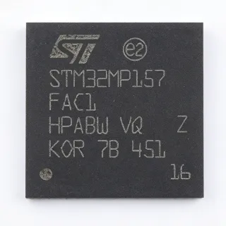
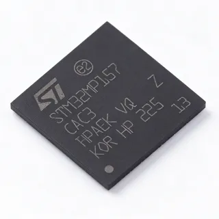
MPC8548EVTATGB - PowerQUICC III e500 MPU, 1.2 GHz | NXP
부품 번호: MPC8548EVTATGB ✓ 활성| 수량 | 단가 | 합계 |
|---|---|---|
| 1 | $176.42 | $176.42 |
| 10 | $172.5 | $1,725.00 |
| 100 | $166.2 | $16,620.00 |
| 500 | $161.4 | $80,700.00 |
| 1,000 | $158.75 | $158,750.00 |
MPC8548EVTATGB 개요
A PowerQUICC III processor is a system-on-chip (SoC) communications engine designed for networking, telecom, and embedded infrastructure equipment. Within the broader taxonomy, it sits at the intersection of microprocessor (MPU) and SoC platform - built on Power Architecture technology with on-chip peripherals that traditionally would require a separate chipset. This category targets high-throughput, deterministic packet and signal-plane processing rather than general-purpose compute.
Key features include 512 KB of internal SRAM, hardware-accelerated cryptography (AES, 3DES, SHA-1/MD5, Kasumi), RAIDEngine XOR acceleration for storage, and a 64-bit DDR1/DDR2 SDRAM memory controller with ECC support. The advanced interrupt controller and four 32-bit timers deliver deterministic real-time response for protocol stacks. Operating voltage domains at 1.0 V core and 1.8 V / 2.5 V / 3.3 V I/O simplify integration into 3.3 V-tolerant backplane designs.
The MPC8548EVTATGB engineering designation (suffix ATGB = 1.2 GHz, industrial temperature, lead-free FCBGA) places it in the higher-performing tier of the MPC8548 family. Pin-compatible variants like the MPC8547 and MPC8572 series share the same FCBGA-783 footprint with reduced or enriched peripheral mixes, enabling designers to migrate up or down without PCB rework. The device implements SMP- and AMP-capable coherency through its CoreNet-compatible interconnect on later derivatives.
Typical applications include multiservice routers, enterprise Layer 2/3 switches, wireless base stations, security appliances, RAID storage controllers, and industrial control planes. The combination of cryptographic acceleration, packet processing, and PCI Express host makes it well-suited for unified threat management (UTM) and IPSec-aware gateways where throughput per watt is critical.
When designing with this device, allocate ample PCB layers (typically 8-12) for FCBGA breakout, maintain DDR2 trace length matching within 25 mils, and sequence the 1.0 V core supply only after the 1.8 V auxiliary rail to avoid latch-up. A JTAG header compliant with IEEE 1149.1 is required for boundary-scan and code-load diagnostics. Watch thermal performance carefully - at 1.2 GHz the device dissipates approximately 8-12 W and benefits from airflow at the board edge.
This page synthesizes distributor pricing, parametric drop-in alternatives within the PowerQUICC III family, and PCB layout guidance beyond what is duplicated in the manufacturer datasheet summary.
드롭인 대체품: MPC8548EVTATGB — 동일 패키지, 핀 호환. PCB 재작업이 필요한 다른 패키지 부품은 제외됩니다.
이 시리즈의 변형
다음과 드롭인 호환되는 동일 시리즈 모델: MPC8548EVTATGB (동일 폼 팩터 및 풋프린트) — 차이점: Core Architecture, RoHS Status, Maximum Core Frequency, Memory Controller, Operating Temperature.
빠른 비교 도구 — 나란히 비교할 대체 부품을 선택하십시오:
MPC8547VTAQGB
✅ 드롭인✓ 재고 있음
$72.4 / 개
데이터시트 보기 →MPC8547EVTAUJB
✅ 드롭인✓ 재고 있음
$124.5 / 개
데이터시트 보기 →MPC8545VTAQGB
✅ 드롭인✓ 재고 있음
$115.4 / 개
데이터시트 보기 →MPC8548ECVTAQGB
✅ 드롭인✓ 재고 있음
$107.48 / 개
데이터시트 보기 →MPC8572ECVTAULE
✅ 드롭인📋 참조 대체품 (카탈로그에 없음)
MPC8548EVTATGB 최대 정격 & 전기적 특성
| Manufacturer | NXP Semiconductors (formerly Freescale) |
| Product Family | PowerQUICC III (MPC85xx) |
| Core Architecture | PowerPC e500 (32-bit superscalar) |
| Number of Cores | 1 |
| Maximum Core Frequency | 1.2 GHz |
| 패키지 | 783-FCBGA (29x29 mm) |
| 실장 유형 | Surface Mount |
| Supply Voltage - Core | 1.0 V |
| Supply Voltage - I/O | 1.8 V / 2.5 V / 3.3 V |
| 동작 온도 | -40C to +105C (industrial grade, AT suffix) |
| L1 Cache (per core) | 32 KB instruction + 32 KB data |
| On-chip SRAM | 512 KB |
| Memory Controller | DDR1/DDR2 SDRAM, 64-bit with ECC |
| Ethernet MAC | 4x 10/100/1000 Mbps (SGMII/RGMII/TBI) |
| High-speed Serial I/O | PCI Express x4, Serial RapidIO 1.2, 2x SGMII |
| Security Engine | AES, 3DES, SHA-1, MD5, Kasumi acceleration |
| RAID Acceleration | RAIDEngine XOR |
| Process Technology | 90 nm CMOS |
| RoHS 상태 | Compliant (lead-free PB-free) |
| Lifecycle | Active - Not recommended for new designs at tail of family |
MPC8548EVTATGB 783-fcbga (29x29 mm) 핀 구성 가이드
MPC8548EVTATGB(783-fcbga (29x29 mm) 패키지)의 핀 구성입니다. 이 디지털 IC에는 GPIO, 통신 인터페이스(UART, SPI, I2C), 전원 핀이 포함되어 있습니다. 대체 핀 기능과 구성 옵션은 제조사 데이터시트를 참조하십시오. 임베디드 시스템 설계와 PCB 레이아웃에 필수적입니다.

다음에 대한 상세 핀아웃 데이터 없음: MPC8548EVTATGB.
다음을 참조하십시오: 데이터시트 전체 핀 구성은 다음을 참조하십시오.
일반적인 애플리케이션
MPC8548EVTATGB 적합 용도: 6 애플리케이션s: Multiservice Routers and Edge Gateways, Enterprise Layer 2/3 Managed Switches, Unified Threat Management (UTM) and IPSec Gateways, Wireless Base Station (BTS/eNodeB) Controllers, RAID and Network-Attached Storage Controllers, Industrial Control and Process Automation.
Multiservice Routers and Edge Gateways
The MPC8548EVTATGB is widely deployed in multiservice routers because it combines a 1.2 GHz e500 core for control-plane routing (OSPF, BGP, IS-IS) with four Gigabit Ethernet MACs and hardware cryptographic acceleration. In a typical edge-router chassis, the device terminates WAN-facing encrypted sessions (IPSec/SSL) at near-line-rate thanks to the integrated AES/SHA hardware engine running at over 1 Gbps bulk throughput, and the PCI Express x4 interface connects to a downstream ASIC for 10G/40G uplink aggregation. Two SGMII lanes support base-T copper PHYs (or 1000BASE-T) directly, and the DDR2 controller provides ample headroom for routing-table memory. The 1.0 V core and 1.8 V/3.3 V I/O simplify integration with a 3.3 V backplane while minimizing core-side dynamic power. This combination explains why NXP promotes the MPC8548EVTATGB as a primary MPU for edge and branch-office networking appliances.
추천
Enterprise Layer 2/3 Managed Switches
For enterprise managed switches, the MPC8548EVTATGB provides a powerful control-plane processor that runs the management stack, runs LACP/SNMP/RMON agents, and bridges to external switch ASICs. The integrated PCI Express x4 interfaces to the data-plane ASIC at 2 GB/s, while the four Gigabit Ethernet MACs can be used for stacking links, management uplinks, or direct copper PHY integration via RGMII/SGMII. The hardware RAIDEngine XOR accelerates storage operations when the switch has local logging. The FCBGA-783 package (29x29 mm) requires 8-12 layer PCB stackup with via-in-pad escape for the 1.0 mm pitch BGA, a layout well-understood by switch OEMs. At 1.2 GHz with full SerDes activity, the device dissipates approximately 8-12 W and requires forced airflow at chassis edges.
추천
Unified Threat Management (UTM) and IPSec Gateways
In UTM gateways and enterprise firewall appliances, the MPC8548EVTATGB accelerates AES-128/192/256, 3DES, SHA-1, MD5, and Kasumi in hardware while the e500 core runs the control-plane OS (Linux, VxWorks, or INTEGRITY). Combined IPSec + deep-packet-inspection throughput typically exceeds 1 Gbps for typical enterprise packet sizes, putting the MPC8548EVTATGB at the heart of branch-office UTM appliances from vendors including SonicWall, Fortinet, and Check Point legacy families. The 64-bit DDR2 ECC memory controller ensures reliable encryption state under backpressure, and the four Ethernet MACs separate management, WAN, LAN, and HA-cluster interfaces. The 1.0 V / 1.8 V / 3.3 V I/O simplifies integration with discrete Ethernet transceivers and crypto co-processors, while the industrial temperature range (-40 C to +105 C junction) supports outdoor deployment of 5G mobile-security appliances.
추천
Wireless Base Station (BTS/eNodeB) Controllers
Wireless base-station baseband units (BBUs) employ the MPC8548EVTATGB to terminate Layer 2/Layer 3 protocol stacks (S1/X2 interfaces in LTE or Iub in 3G) and to schedule cell-site Ethernet traffic. The Kasumi cryptographic engine provides the bulk encryption needed for 3GPP air-interface ciphering as data moves between the backhaul and the radio head. Serial RapidIO 1.2 links the BBU to a baseband modem ASIC at distances up to tens of centimeters on the same backplane, while PCI Express connects to the radio front-end (CPRI) converter. The four Ethernet MACs support L2/L3 backhaul, synchronization (SyncE / IEEE 1588), and S1-AP/S1-U traffic. Industrial temperature grading (-40 C to +105 C) is well-suited to outdoor cabinet installations where ambient temperatures can swing widely.
추천
RAID and Network-Attached Storage Controllers
Network-attached storage (NAS) controllers and RAID HBAs leverage the MPC8548EVTATGB's integrated RAIDEngine XOR acceleration for RAID 5/6 parity calculations. The device handles file-system metadata, iSCSI offload (combined with software stack), and SAS/SATA expansion via downstream controllers on PCI Express. Four Gigabit Ethernet MACs allow multi-port NAS appliances to service clients and back-end replication without external switches. The 64-bit DDR2 ECC controller ensures data integrity under heavy I/O workloads, and 512 KB of on-chip SRAM provides caching for control structures. Layered with a hardware hash engine for SHA-1/MD5, the platform can validate file-system metadata at line rate during scrubs and rebuilds.
추천
Industrial Control and Process Automation
Industrial gateways, substation routers, and process-automation controllers adopt the MPC8548EVTATGB for its deterministic Book-E interrupt latency, industrial temperature range (-40 C to +105 C junction), and long-term availability through NXP's product longevity program. PCI Express and Serial RapidIO link to I/O cards for deterministic control loops, while multiple Gigabit Ethernet MACs handle ring topologies using IEC 62439 PRP/HSR for substation automation. The 783-FCBGA package mates well with the ruggedized PCB stackups typical of industrial designs (8+ layers, controlled-impedance routing). DDR2 ECC memory provides single-bit error correction needed for high-availability applications in power-grid protection relays.
추천
추천 제품 요약
엔지니어링 참조 데이터: MPC8548EVTATGB — 비교, 설계 지침 및 규정 준수 정보.
선택 가이드
대체품과의 비교
| 파라미터 | 이 제품 | MPC8547VTAQGB | MPC8547EVTAUJB | MPC8545VTAQGB | MPC8548ECVTAQGB | MPC8572ECVTAULE |
|---|---|---|---|---|---|---|
| Package | 783-FCBGA (29x29 mm) | 783-FCBGA (29x29 mm) | 783-FCBGA (29x29 mm) | 783-FCBGA (29x29 mm) | 783-FCBGA (29x29 mm) | 783-FCBGA (25x25 mm) |
| Brand | NXP Semiconductors | NXP Semiconductors | NXP Semiconductors | NXP Semiconductors | NXP Semiconductors | NXP Semiconductors |
| Core Frequency | 1.2 GHz | 1.0 GHz (-17%) | 1.0 GHz (-17%) | 1.0 GHz (-17%) | 1.0 GHz (-17%) | 1.333 GHz (+11%, dual core) |
| Core Architecture | e500 single core | e500 single core | e500 single core | e500 single core | e500 single core | e500 dual core |
| Gigabit Ethernet MACs | 4 | 4 | 4 | 3 | 4 | 4 |
| Security Engine | Enabled (AES/3DES/SHA/Kasumi) | Enabled | Disabled | Enabled | Enabled | Enabled |
| SerDes Lanes | x4 PCIe + 2 SGMII + sRIO | x4 PCIe + 2 SGMII + sRIO | x4 PCIe + 2 SGMII + sRIO | x4 PCIe + 2 SGMII | x4 PCIe + 2 SGMII + sRIO | x4 PCIe + 4 SGMII |
| Memory Controller | DDR1/DDR2 64-bit ECC | DDR1/DDR2 64-bit ECC | DDR1/DDR2 64-bit ECC | DDR1/DDR2 64-bit ECC | DDR1/DDR2 64-bit ECC | DDR1/DDR2 64-bit ECC |
| Operating Temperature | -40C to +105C (industrial) | -40C to +105C | -40C to +125C | -40C to +105C | -40C to +105C | -40C to +105C |
| Lifecycle / Availability | Active, mature | Active, mature | Active, mature | Active, mature | Active, mature | Active, mature |
주요 차별점
- Highest CPU frequency in the MPC8548 family (vs MPC8547VTAQGB)
- Full security engine enabled at production silicon revision (vs MPC8547EVTAUJB)
- Single e500 core optimized for control-plane (vs MPC8572ECVTAULE)
- Industrial temperature range (-40 C to +105 C) (vs MPC8547VTAQGB)
설계 노트
The 783-FCBGA at 1.0 mm pitch demands a microvia escape pattern. Use an 8-12 layer PCB stackup with HDI (AnyLayer microvia) construction, 0.5 oz copper on outer layers, 1 oz on inner power planes, and a dedicated ground plane beneath the BGA. Assign distinct reference planes for the 1.0 V core, 1.8 V DDR2 VTT, and 2.5 V / 3.3 V I/O to reduce return-path stitching concerns.
At 1.2 GHz with all SerDes lanes active, the MPC8548EVTATGB dissipates approximately 8-12 W. Estimate junction temperature as TJ = TA + (PD x theta_JA). With typical theta_JA of 12 C/W on a 12-layer board and 1.5 m/s forced air, derate to keep TJ below 105 C industrial limit. Heatsink attachment should use a thermal interface material with conductivity >= 1.0 W/m-K and avoid covering the FCBGA ball array beneath the lid.
DDR2 interface requires length matching within 25 mils for byte lanes and within 50 mils across the 64-bit data bus. Use fly-by topology with VTT termination at the farthest DIMM socket. Route the 1.8 V VTT as a 1.8 V island with 0.1 uF decoupling every 5 mm along the bus. The clock pair (CK/CKn) requires differential 100-ohm impedance and a far-end termination at the DIMM.
Power-up sequencing must apply 1.0 V core only after the 1.8 V AUX rail reaches specification, per datasheet recommendation. Use a UCD9090 or PMBus-compatible sequencer for production designs; for low-volume, an RC timer driving a load switch is acceptable. Add 10 uF bulk + 0.1 uF HF decoupling on each rail, with the 0.1 uF placed within 5 mm of the BGA balls. Soft-start ramp of the 1.0 V core should be limited to 30 ms maximum.
Do not populate PCI Express Lanes 1-3 on the same channels as Serial RapidIO - they share SerDes multiplex logic and cannot operate simultaneously. Configure the SerDes protocol mode during POR via the cfg_rcw[0:7] boot source. Common boot faults arise from mismatched PCI Express reset topology; ensure PERST# is held low until the core PLL is locked.
규정 준수 정보
PB-free designation per suffix 'PB Free'. RoHS compliant per EU Directive 2011/65/EU and (EU) 2015/863. Industrial temperature grade (AT suffix) - not AEC-Q100 automotive.