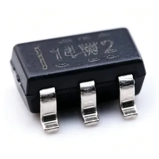
OPA378AIDBV - Zero-Drift 900kHz RRIO Op Amp | TI
MPN: OPA378AIDBV ✓ NakahandaOPA378AIDBV Ulas
A zero-drift operational amplifier (also called a chopper-stabilized or auto-calibrated amplifier) is a precision amplifier topology that uses internal switching and correction to continuously null its input offset voltage, eliminating the 1/f (flicker) noise and offset drift that limit DC accuracy in conventional CMOS or bipolar op amps. The OPA378 belongs to the broader family of operational amplifiers -> precision amplifiers -> amplifiers -> analog signal-chain ICs -> semiconductor devices. This category is critical whenever a circuit needs to amplify or buffer microvolt-level DC signals without drift across temperature.
Key specifications include a 900 kHz gain bandwidth product (GBW), 2.5 V/us typical slew rate, RRIO operation from a 2.7 V to 5.5 V single supply, 150 uA maximum quiescent current, and an input bias current of 200 pA. The combination of low offset (20 uV), near-zero drift (0.1 uV/°C), low noise, and micropower consumption enables high DC accuracy in battery-powered and bridge-sensor applications without auto-zero cycle latency.
Internally, the OPA378 uses a proprietary auto-calibration technique that continuously samples and corrects the input stage offset, achieving picoampere-level effective input bias drift over time and temperature. Rail-to-rail input and output stages allow the part to operate with signals that approach either supply rail, maximizing dynamic range in low-voltage single-supply systems. The 5-pin SOT-23 package is footprint-compatible with industry-standard SOT-23-5 single-channel op amps, supporting PCB-level drop-in replacement.
Typical applications include precision strain-gauge and thermocouple signal conditioning, transducer excitation amplifiers, battery-powered sensor front-ends, medical instrumentation, handheld test equipment, and current-sense amplifiers. Designers select the OPA378 specifically when sub-100 uV DC error and sub-uV/°C drift are required in systems that cannot tolerate the noise and quiescent current of legacy precision op amps.
When designing with this device, ensure the input common-mode range includes the expected signal excursion, since RRIO operation only guarantees linear behavior within the specified input voltage range. Use low-impedance drive sources or a series input resistor to attenuate switching transients from the chopper front-end, and add a small RC filter at the output if any residual clock feedthrough is unacceptable in the target application.
This page synthesizes distributor pricing, drop-in alternatives, and practical design notes not found in the manufacturer datasheet, giving engineers an actionable reference for sourcing and second-sourcing decisions.
Mga alternatibo na pwedeng ilagay na OPA378AIDBV — parehas na package, pin-to-pin na katugmang. Hindi kasama ang mga bahagi ng iba't-ibang package na nangangailangan ng pagpapaayos ng PCB.
Variante sa Seri na ito
Katulad na modelo sa serye na katugma sa pagpasok OPA378AIDBV (parehas na form factor at footprint) — pagkakaiba sa MSL Level, Number of Channels, Operating Temperature Range, Package.
OPA378AIDBVR
✅ Drop-In📋 Alternatibo na Reference (hindi sa katalogo)
OPA2378AIDGKR
✅ Drop-In ⚠️ Mga Talaan Hindi Naiwerikmo📋 Alternatibo na Reference (hindi sa katalogo)
MAX44250AUT+T
✅ Drop-In📋 Alternatibo na Reference (hindi sa katalogo)
MAX9914EXK+T
✅ Drop-In📋 Alternatibo na Reference (hindi sa katalogo)
LMV841MGX/NOPB
✅ Drop-InMagkontak para sa presyo
Tingnan ang Datasheet →OPA378AIDBV Mga Pinakamataas na Rating at Electrical Characteristics
| Manufacturer | Texas Instruments |
| Product Type | Zero-Drift Precision Operational Amplifier |
| Number of Channels | 1 |
| Gain Bandwidth Product (GBW) | 900 kHz |
| Slew Rate | 2.5 V/us (typical) |
| Input Offset Voltage (Vos) | 20 uV (maximum) |
| Offset Voltage Drift (dVos/dT) | 0.1 uV/°C |
| Quiescent Current (Iq) | 150 uA (maximum) |
| Input Bias Current (Ib) | 200 pA |
| Supply Voltage Range (Vs) | 2.7 V to 5.5 V (single supply) |
| Input/Output Type | Rail-to-Rail Input and Output (RRIO) |
| Hanay ng Temperature na Operasyon | -40°C to +125°C |
| Packhaging | SOT-23-5 (DBV) |
| Uri ng Pagpapasok | Surface Mount |
| Level ng MSL | 1 (unlimited) |
| Tindminan RoHS | Compliant |
| AEC-Q100 Qualified | No (industrial grade only) |
Pin Configuration ng OPA378AIDBV
| Pin 1 | NC / Offset Trim — No-connect (offset trim pin left floating for standard use) |
| Pin 2 | -In — Inverting input |
| Pin 3 | +In — Non-inverting input |
| Pin 4 | V- / GND — Negative supply (ground for single supply) |
| Pin 5 | V+ — Positive supply (2.7 V to 5.5 V) |
Tipikal na mga Gamit
OPA378AIDBV ay nararapat para sa 6 aplikasyons: Strain-Gauge / Load-Cell Signal Conditioning, Thermocouple / Cold-Junction Compensation, Battery-Powered Sensor Front-End, Medical Instrumentation Amplifier, Precision Current-Shunt Amplifier, Handheld Test & Measurement Equipment.
Strain-Gauge / Load-Cell Signal Conditioning
The OPA378AIDBV's 20 uV maximum input offset voltage and 0.1 uV/°C drift make it ideal for strain-gauge bridge amplifiers where microvolt-level differential signals must be amplified without thermal drift over the -40°C to +125°C range. Placed in the first gain stage with a fixed gain of 100, the part converts a full-scale bridge output of 1 mV/V to a 10 mV signal with sub-50 uV total error, eliminating the need for periodic system recalibration.
Inirekomenda
Thermocouple / Cold-Junction Compensation
For thermocouple front-ends measuring microvolt-per-degree Celsius signals, the OPA378AIDBV's zero-drift architecture and 200 pA input bias current reject 1/f noise and thermal EMF buildup at the thermocouple junction. Used as a low-noise front-end with a gain of 50-100 followed by a precision ADC, the part achieves better than 0.1°C measurement repeatability across the K-type thermocouple range (-200°C to +1372°C) without chopper feedthrough artefacts.
Inirekomenda
Battery-Powered Sensor Front-End
The OPA378AIDBV's 150 uA maximum quiescent current and 2.7 V-5.5 V supply range make it ideal for battery-powered IoT and portable sensor nodes where every microwatt of bias current matters. Combined with rail-to-rail I/O for maximum dynamic range at low supply voltages, the part delivers precision DC amplification for current-sense, voltage-sense, or analog-output sensors while preserving battery life for multi-year deployments.
Inirekomenda
Medical Instrumentation Amplifier
In ECG, EEG, and bio-impedance front-ends, the OPA378AIDBV's 20 uV Vos and 0.1 uV/°C drift ensure that millivolt-level bioelectric signals are amplified faithfully across patient body temperature variations and ambient shifts. Used as the input stage of a three-op-amp instrumentation amplifier with 0.1% gain-set resistors, the part supports medical-grade measurement with sub-mV error budgets in wearable and diagnostic platforms.
Inirekomenda
Precision Current-Shunt Amplifier
For high-side or low-side current-sense circuits reading across a 10-100 mΩ shunt, the OPA378AIDBV's low Vos drift across temperature eliminates current measurement error when the surrounding power electronics heat up. Used with a fixed gain of 20-50 to convert a 0-100 mV shunt signal to a 0-5 V ADC input, the zero-drift topology avoids the 0.3-3 uV/°C drift inherent in standard op amps which would otherwise demand temperature calibration.
Inirekomenda
Handheld Test & Measurement Equipment
In portable multimeters, low-bandwidth oscilloscopes, and signal calibrators, the OPA378AIDBV's combination of low offset (20 uV), high GBW (900 kHz), and rail-to-rail I/O enables precise buffer and gain stages that operate from a single Li-ion cell. The 5-pin SOT-23 package minimizes PCB area in handheld enclosures, while the 150 uA quiescent current extends battery runtime between charges.
Inirekomenda
Buod ng mga Inirekomendang Produkto
Impormasyon ng Talumpati sa Engineering for OPA378AIDBV — ikabit, gabay sa disenyo, at impormasyon ng pagsunod sa kautusan.
Paunawang Hanapin
Ikabit sa Mga Alternatibo
| Parametro | Ito ang Producto | OPA378AIDBVR | OPA2378AIDGKR | MAX44250AUT+T | MAX9914EXK+T | LMV841MGX/NOPB |
|---|---|---|---|---|---|---|
| Brand | Texas Instruments | Texas Instruments | Texas Instruments | Analog Devices (Maxim) | Analog Devices (Maxim) | Texas Instruments |
| Package | SOT-23-5 (DBV) | SOT-23-5 (DBV) | MSOP-8 (DGK) - dual, different footprint | SOT-23-5 | SC-70-5 (slightly smaller) | SC-70-5 (MGX) |
| Gain Bandwidth Product | 900 kHz | 900 kHz | 900 kHz | 10 MHz (much higher) | ~500 kHz | 4.5 MHz |
| Quiescent Current (max) | 150 uA | 150 uA | 150 uA per channel | 1.2 mA (higher) | ~200 uA | 1.5 mA |
| Supply Voltage Range | 2.7 V to 5.5 V | 2.7 V to 5.5 V | 2.7 V to 5.5 V | 2.7 V to 5.5 V | 2.7 V to 5.5 V | 2.7 V to 5.5 V |
| Rail-to-Rail I/O | Yes (RRIO) | Yes | Yes | Yes | Yes | Output only (no RRIO) |
Pangunahing mga Pagkakaiba
- Sub-uV/°C drift eliminates thermal calibration (kumpara saLMV841MGX/NOPB)
- Single-supply RRIO operation maximizes dynamic range at low Vs (kumpara saMAX9914EXK+T)
- Pin-compatible drop-in versus the dual OPA2378 sibling for designs needing second-source (kumpara saOPA2378AIDGKR)
Talaan ng Disenyo
Estimated: source impedance above 10 kΩ injected into the +In/-In pins can interact with the auto-calibration switches and amplify residual clock feedthrough as a DC offset error. For a strain-gauge bridge with 1 kΩ output impedance this is rarely a problem, but for thermocouples with 10 kΩ source resistance add a unity-gain buffer at the input. The TI OPA378 datasheet (Rev. D) recommends keeping source impedance below 1 kΩ for lowest drift, otherwise add a series RC filter (10 kΩ + 1 nF) to roll off chopper transients.
Estimated: the SOT-23-5 thermal pad is on pin 4 (V-/GND), so use a small copper pour connected to ground to improve thermal dissipation when operating near 150 uA quiescent at +125°C ambient. Place a 0.1 uF X7R bypass capacitor within 2 mm of the V+ pin and a 10 uF tantalum or ceramic bulk capacitor at the supply node; keep input traces short and parallel to reduce loop area and avoid sourcing noise into the high-impedance inputs. Ground-plane stitching every 5 mm under the input traces lowers stray pickup in RF or switching environments.
For precision designs, route the inverting and non-inverting inputs as a matched differential pair on the same layer with constant 0.2-0.3 mm spacing to reject thermal and capacitive gradients. Place any gain-setting feedback resistors immediately next to the inverting input and connect their far ends to a clean ground pour or to the output pin with minimal trace length. Apply a guard ring driven by the same input signal around high-impedance traces to reduce leakage currents from contaminated PCB surfaces, particularly in presence of flux residues or humidity.
Impormasyon ng Pagsunod sa Kautusan
RoHS compliant per TI product page. Not AEC-Q100 qualified - industrial temperature grade only (-40°C to +125°C). Lead-free and halogen-free per TI's environmental compliance markings.