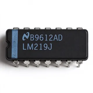
CD4024AD3 - 7-Bit CMOS Binary Counter | Harris | CDIP-14
MPN: CD4024AD3 ✓ AktifCD4024AD3 Genel Bakış
A binary counter is a type of counter IC that stores and advances a multi-bit binary number. The CD4024AD3 uses an asynchronous ripple-carry counting architecture: each output stage changes after the preceding stage, allowing successive binary states to appear across the seven outputs. Negative-edge triggering means the count advances on the high-to-low transition of the clock input rather than its low-to-high transition. This behavior must be considered when defining reset timing and external clock-conditioning circuits.
The principal features of the CD4024AD3 include seven counter outputs, negative-edge clock triggering, asynchronous counting, and operation from 3 V to 12 V. Because it uses CMOS technology, the circuit is suitable for low-voltage digital systems in which supply current, logic thresholds, and integration density are important considerations. The parallel binary outputs provide a direct representation of the current count from 0 through 127, simplifying connections to displays, decoders, programmable controllers, or other digital subsystems.
The 14-CDIP package provides through-hole access to the counter, clock, reset, and output functions. Its lead spacing supports conventional PCB layouts and socketed assemblies rather than fine-pitch surface mounting. Pin assignments should be taken from the Harris CD4024AD3 datasheet when assigning PCB tracks, especially because adjacent counter stages may be brought out in a non-sequential physical order. The asynchronous ripple architecture is straightforward for low-to-moderate clock rates, but propagation delay accumulates through the seven stages and should be checked against the maximum system clock requirement.
Typical uses include digital frequency division, event-counting modules, timing dividers, industrial control logic, laboratory counters, and educational digital-logic systems. The part can divide an incoming pulse train by 2, 4, 8, 16, 32, 64, or 128 by observing the corresponding output stage. It is also useful when a controller requires a binary state that can be read in parallel rather than decoded from a one-hot sequence.
For reliable circuit design, use a clean clock edge and account for cumulative ripple delay before using the most significant output as a high-frequency timing reference. Reset should be asserted long enough to establish a defined starting state, and unused inputs must be held at valid CMOS logic levels. Because a CDIP package exposes long leads, pay particular attention to lead clearance, soldering temperature, and protection from electrostatic discharge during handling.
This product record combines the verified Harris CD4024AD3 ordering description, electrical classifications, package information, sourcing observations, and practical implementation guidance. It also identifies where a true pin-compatible replacement must be confirmed instead of treating a functionally similar counter as an automatic drop-in substitute. Engineers can use the comparison and validation guidance below to evaluate board-level compatibility, timing margins, lifecycle risk, and sourcing requirements before approving an alternative.
Drop-in alternatifler için CD4024AD3 — aynı paket, pin-başına uyumlu. PCB yeniden montajı gerektiren farklı paket bileşenleri dışlanmıştır.
Bu ürüne yer değiştirme seçenekleri mevcut değil.
Alternatifleri Talep EdinCD4024AD3 Maksimum Değerlendirmeler & Elektriksel Özellikler
| Counter Type | Binary asynchronous up counter |
| Number of Counter Elements | 1 element |
| Counter Resolution | 7 bits |
| Clock Edge Sensitivity | Negative edge |
| Logic Level | CMOS |
| Supply Voltage Range | 3 V to 12 V |
| Counting Direction | Up |
| Çıkış Sayısı | 7 binary outputs |
| Maximum Count | 127 |
| Counting Architecture | Asynchronous ripple carry |
| Logic Family | 4000/14000/40000 CMOS series |
| Package Type | 14-CDIP |
| Montaj Türü | Through-hole |
| Lead Spacing | 7.62 mm |
CD4024AD3 14-cdip Pin Yapısı Kılavuzu
CD4024AD3 (14-cdip paket) için pin yapısı. Bu dijital IC, GPIO, iletişim arayüzleri (UART, SPI, I2C) ve güç pinleri içerir. Alternatif pin işlevleri ve yapılandırma seçenekleri için üretici veri kitapçığını referans alın. Tünel sistem tasarımı ve PCB yerleşimi için temel bir bileşendir.

Ayrıntılı pin çıkış verisi mevcut değil: CD4024AD3.
Aşağıdaki veri sayfası tam pin konfigürasyonu için.
Tipik Uygulamalar
CD4024AD3 için uygundur 6 uygulamas: Digital Frequency Divider, Industrial Event Counter, Programmable Timer and Retrigger, Binary State Decoder Interface, Laboratory Pulse-Counting Module, Legacy Digital Control System.
Digital Frequency Divider
The CD4024AD3 works as a programmable frequency divider because its seven counter outputs provide division ratios of 2, 4, 8, 16, 32, 64, and 128. A clock applied to the negative-edge-triggered input advances the asynchronous ripple counter, while the selected Q output produces the divided waveform. This arrangement is useful in timing generators, pulse-rate reducers, and clock-polling systems. The principal design consideration is cumulative propagation delay across the seven stages. For high-ratio outputs, the most significant stage has the greatest settling delay, so verify the maximum source frequency and required output duty-cycle accuracy against the manufacturer timing data before treating the divided signal as a precision reference.
Önerilen
Industrial Event Counter
The CD4024AD3 can count discrete events from sensors, switches, or machine-position encoders and present the total as a seven-bit parallel value. Each accepted negative clock transition advances the count, allowing a controller to read the accumulated state after a defined interval. Its CMOS 3 V to 12 V operating range supports common industrial logic levels, while the 14-CDIP package simplifies through-hole construction and field replacement. In industrial environments, protect switch and sensor inputs from bounce, contact noise, and transients. Reset timing and the maximum event rate must also be checked so that the controller never samples during the ripple transitions of the counter stages.
Önerilen
Programmable Timer and Retrigger
The seven binary outputs of the CD4024AD3 allow a retriggerable timer to be built by combining the counter with combinational decoding logic. A pulse resets the counter, and a decoded output indicates a selected count interval, after which the next clock edge returns the circuit toward its next timing cycle. This approach supports variable delays selected by changing the decode taps. Because the CD4024AD3 is an asynchronous ripple counter, decode transitions can momentarily propagate through more than one state. Debounce or qualify each decoded output if the load must never observe a false pulse, and include the reset-release and clock-period margin in the timing budget.
Önerilen
Binary State Decoder Interface
The CD4024AD3 provides a natural interface between sequential events and parallel logic. Its seven outputs can feed decoders, display drivers, multiplexers, comparators, or programmable controllers that need a binary count rather than a pulse train. A change on a selected clock edge updates the output word, making the device suitable for position-step sequencing and mode selection in control systems. Engineers should sample only after the relevant output stages have settled, or register the outputs in a flip-flop bank. The 14-CDIP outline also makes the counter practical for legacy controller boards where a socketed or repairable logic section is preferable to a fine-pitch surface-mount device.
Önerilen
Laboratory Pulse-Counting Module
The CD4024AD3 can serve as the counting element in a laboratory pulse-counter module, replacing a larger mechanical counter when the input is clean and the required count range does not exceed 127. Its parallel outputs simplify display multiplexing, comparison, and data logging, while the negative-edge trigger can be aligned with pulse sources that define timing on the falling edge. Input conditioning should prevent contact bounce, ringing, and amplitude variations from causing multiple counts. For bench equipment, the through-hole package is convenient to socket, replace, and inspect. Confirm the counter's maximum clock frequency and output settling behavior before using it with fast pulse generators or long cable runs.
Önerilen
Legacy Digital Control System
The CD4024AD3 is appropriate for repair and extension of legacy CMOS control systems that already use 14-CDIP logic and require a binary up-counter. Its 3 V to 12 V supply compatibility supports several generations of transistor-transistor and CMOS logic interfaces, provided signal levels meet the CD4000-family input thresholds. The through-hole package allows direct board-level replacement where a modern surface-mount counter would require layout changes. Engineers should first compare the full pin table, negative-edge triggering, reset polarity, and output order with the failed device. Also review counter speed and temperature specifications because older control boards may be noise-sensitive and operate at elevated temperatures.
Önerilen
Önerilen Ürünler Özeti
Mühendislik referans verileri: CD4024AD3 — karşılaştırma, tasarım rehberi ve uyumluluk bilgileri.
Seçim Kılavuzu
Alternatiflerle Karşılaştırma
| Parametre | Bu Ürün |
|---|---|
| Package | 14-CDIP |
| Brand | Harris Corporation |
| Counter Resolution | 7 bits |
| Counter Elements | 1 element |
| Counting Direction | Up |
| Clock Edge | Negative edge |
| Counting Architecture | Asynchronous ripple carry |
| Logic Technology | CMOS |
| Supply Voltage Range | 3 V to 12 V |
| Maximum Binary Count | 127 |
Ana Farklılayıcılar
- Seven-bit count with parallel binary outputs (karşılaştırma:CD4024AD)
- Defined negative-edge counting behavior (karşılaştırma:CD4024AD)
- Through-hole 14-CDIP construction (karşılaştırma:CD4024AD)
Tasarım Notları
Treat the CD4024AD3 clock as a sensitive asynchronous timing input. Keep the driver close to the clock pin, use a short return path, and avoid routing the clock beside noisy switching nodes. If the source is mechanical or a long cable, add conditioning to prevent contact bounce, ringing, and multiple negative-edge detections. The triggering edge is specifically negative, so the timing diagram must align reset and source pulses with the falling transition rather than assuming rising-edge behavior.
Assign every connection from the Harris CD4024AD3 pin-description table rather than assuming that Q0 through Q6 appear in numerical order around the 14-CDIP outline. Route the seven outputs according to their logical function and keep clock and reset traces away from sensitive analog or high-current switching paths. Use a ground plane where practical, place input conditioning close to the clock pin, and provide local supply bypassing. The long CDIP leads make careful lead-bend radius and soldering practice important during manual assembly.
Do not sample the binary outputs immediately after a clock edge if the downstream circuit requires a settled word. Asynchronous ripple propagation means the seven stages do not change simultaneously. Add a sampling delay, register the outputs, or decode only stages that have met their settling requirements. Also verify reset polarity and minimum reset duration from the manufacturer datasheet. A reset that is too short may leave different stages in different states, producing an invalid intermediate count.
The verified device specification establishes a 3 V to 12 V operating range, but maximum input-current, dynamic-current, and power-dissipation figures are not stated in the product record. Before committing to a supply rail, review those characteristics in the manufacturer datasheet and include CMOS transition-current demand from all seven outputs. Place the decoupling capacitor at the device supply pins, maintain a low-impedance return path, and avoid sharing a long supply route with unrelated switching loads that could produce rail disturbance during count transitions.
Uyumluluk Bilgisi
The Harris CD4024AD3 product description does not provide RoHS, REACH, lead-free, halogen-free, conflict-minerals, or automotive-qualification declarations. AEC-Q100 status is recorded as not qualified because this legacy CMOS logic device is not identified as an automotive-qualified variant.