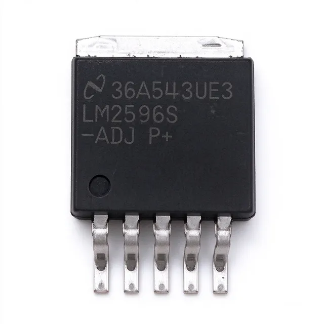
LM2596S-ADJ - 3A Adjustable Step-Down Switcher | Texas Instruments
MPN: LM2596S-ADJ ✓ AktifLM2596S-ADJ Genel Bakış
A buck (step-down) switching regulator is a type of DC-DC converter that uses a power switch, inductor, and rectifier to efficiently lower an input voltage to a lower regulated output. Compared with linear regulators, buck converters dissipate far less power because they switch the pass element fully on or fully off, reaching typical efficiencies of 73% to 88% at 3 A. The LM2596 sits in the classic SIMPLE SWITCHER family: non-isolated, asynchronous, and easy to design around with standard 33 µH inductors and 220 µF output capacitors.
Key features include a fixed 150 kHz internal oscillator, 3 A continuous output current, 4.5 V to 40 V input range, adjustable output from 1.2 V to 37 V (set by external feedback resistors), TTL-shutdown input, internal current limiting, and thermal shutdown. The 5-lead TO-263 (D2PAK) tab provides a low thermal-resistance path that can dissipate the 7 W to 15 W typical full-load losses when soldered to sufficient copper area.
Internally, the LM2596 uses a fixed-frequency, peak-current-controlled control architecture with an external compensation network chosen by the output capacitor type. The datasheet specifies standard and high-efficiency design tables that pair 33 µH inductors with 220 µF output capacitors (standard) or 330 µF with Schottky rectifiers (high-efficiency), giving the designer a proven starting BOM.
Typical applications include 24 V-to-5 V/3.3 V industrial bus conversion, automotive accessory power, hobby robotics and drone LiPo battery regulation, distributed 12 V PoE auxiliary rails, and DIY buck modules. With thousands of third-party modules built around the part, it remains the canonical first buck regulator most engineers cut their teeth on.
When designing, follow the datasheet catch-diode selection carefully: a 3 A Schottky such as the MBR360 keeps efficiency high, while a 1N5822 or similar is acceptable for lower-frequency, lower-cost designs. Keep the input capacitor loop tight and never operate above 40 V input; add a TVS such as P6KE39A for transients beyond 40 V.
This page synthesizes distributor pricing, drop-in alternatives, and practical design notes not found in the manufacturer datasheet alone, giving engineers a single decision-ready view of the LM2596S-ADJ.
Drop-in alternatifler için LM2596S-ADJ — aynı paket, pin-başına uyumlu. PCB yeniden montajı gerektiren farklı paket bileşenleri dışlanmıştır.
Bu Serideki Variantlar
Yedek parça uyumlu olan aynı serideki modeller LM2596S-ADJ (aynı form faktörü ve ayağa oturma) — farklı olan Package, RoHS Status, Switching Frequency, Input Voltage Range, Efficiency.
LM2596SX-ADJ/NOPB
Fiyat için iletişime geçin
Veri Şablonunu Görüntüle →LM2596S-ADJ/NOPB
📋 Katalogda Olmayan Referans Alternatifi
LM2596HV-ADJ
📋 Katalogda Olmayan Referans Alternatifi
XL2596S-ADJ
📋 Katalogda Olmayan Referans Alternatifi
LM2576S-ADJ
📋 Katalogda Olmayan Referans Alternatifi
GS2596-ADJ
📋 Katalogda Olmayan Referans Alternatifi
LM2596S-ADJ Maksimum Değerlendirmeler & Elektriksel Özellikler
| Ağ Yapısı | Buck (Step-Down) |
| Çıkış Türü | Adjustable |
| Çıkış Gerilimi Aralığı | 1.2 V to 37 V |
| Maksimum Çıkış Akımı | 3 A |
| Giriş电压范围 | 4.5 V to 40 V |
| Değiştirme Frekansı | 150 kHz (fixed, internal oscillator) |
| Geri Bildirim Voltage | 1.23 V (typical internal reference) |
| Durağan Akım | 5 mA (typical, switching) |
| Standby Current (Shutdown) | 50 µA (typical) |
| Verimlilik | 73% to 88% (typical, depends on VIN/VOUT/load) |
| İşletim Sıcaklığı Aralığı | -40 °C to +125 °C |
| Paket | TO-263-6, D2PAK (5 Leads + Tab), TO-263BA |
| Montaj Türü | Surface Mount |
| MSL Seviyesi | 3 |
| RoHS Durumu | Compliant (lead-free LM2596S-ADJ/NOPB variant) |
LM2596S-ADJ Pin Yapısı
| Pin 1 | VIN — Input supply voltage (4.5 V to 40 V) |
| Pin 2 | OUTPUT — Switch node - connects to inductor and catch diode |
| Pin 3 | GND — Ground reference |
| Pin 4 | FEEDBACK — Feedback voltage input (1.23 V reference), set by resistor divider |
| Pin 5 | ON/OFF — TTL shutdown input (logic-low enables regulator) |
| Pin 6 | TAB (GND) — Exposed tab - internally tied to GND, solder to PCB copper for heatsinking |
Tipik Uygulamalar
LM2596S-ADJ için uygundur 6 uygulamas: 24 V Industrial Bus to 5 V / 3 A Conversion, Automotive 12 V Accessory Power, Hobby Robotics / Drone LiPo Regulation, Distributed 12 V PoE Auxiliary Rails, DIY Buck Modules / Blue LM2596 Buck Boards, Solar Charge Controller Auxiliary Loads.
24 V Industrial Bus to 5 V / 3 A Conversion
The LM2596S-ADJ's 4.5 V to 40 V input range and 3 A output make it the canonical buck converter for 24 V industrial bus systems. Per the TI datasheet design tables, with VIN = 24 V, VOUT = 5 V at 3 A, the regulator hits ~80% efficiency with a 33 µH inductor and MBR360 Schottky; the TO-263 tab dissipates 5-7 W into a 6 cm² copper pour. Engineers value the regulator for PLC I/O, sensor hubs, and motor-driver auxiliary rails because it requires only four external parts, has internal current limit and thermal shutdown, and survives 40 V transients without external TVS.
Önerilen
Automotive 12 V Accessory Power
For automotive 12 V battery systems running accessories (LED light bars, fans, USB chargers), the LM2596S-ADJ is well suited because its 40 V input rating covers load-dump transients (with a TVS), and the adjustable output can be set from 1.2 V up to 13 V. Per the TI datasheet, a 12 V-to-5 V / 3 A accessory rail delivers ~85% efficiency with 33 µH/220 µF standard BOM. Add a P6KE39A TVS at the input to clamp load-dump events above 40 V, and place a 470 µF input capacitor to survive cold-crank dips below 6 V.
Önerilen
Hobby Robotics / Drone LiPo Regulation
Hobby robotics, drones, and RC vehicles often need 5 V or 12 V rails from a 3 S / 4 S LiPo (12.8 V nominal up to 16.8 V full). The LM2596S-ADJ accepts up to 40 V, so it can ride through the LiPo voltage range while delivering 3 A to servos, BEC circuits, or auxiliary boards. Per the TI datasheet, a 4 S-to-5 V / 3 A supply runs at ~78% efficiency with a 68 µH inductor; pair the TO-263 tab to a small copper pad (~4 cm²) to handle the 8-10 W dissipation during high throttle events.
Önerilen
Distributed 12 V PoE Auxiliary Rails
PoE-powered devices need isolated or non-isolated auxiliary rails for fans, LEDs, and control logic. The LM2596S-ADJ handles the post-PoE 12 V bus well, stepping it down to 5 V / 3 A at ~85% efficiency for fan and LED drivers per the TI datasheet design tables. With 33 µH inductor and 220 µF capacitors it forms a stable, low-noise rail; the TO-263 footprint drops onto a 4-layer PoE board alongside the isolated PoE PD controller.
Önerilen
DIY Buck Modules / Blue LM2596 Buck Boards
The LM2596S-ADJ is the regulator behind the famous blue 4-pin 'buck converter' modules sold worldwide (In, Out+, Out-, EN). These modules accept 4-40 V, deliver 1.25-35 V at 3 A, and are calibrated with an external multi-turn pot on the feedback divider. Per the TI datasheet BOM, a 33 µH inductor, 470 µF input cap, 220 µF output cap, and MBR360 Schottky form the complete module. The TO-263 tab is soldered to the module's exposed copper pour for heat spreading.
Önerilen
Solar Charge Controller Auxiliary Loads
Off-grid solar charge controllers often run from a 24 V battery bus that swings from 20 V to 30 V and must power 5 V / 12 V loads (display, fan, MCU rails). The LM2596S-ADJ is an excellent choice: 40 V input margin covers 30 V battery + transient spikes, 3 A output handles fan + MCU + relay coils, and the TO-263 tab dissipates the 5-10 W losses to PCB copper. Per TI datasheet, a 24 V-to-5 V design runs at ~80% efficiency; a 24 V-to-12 V rail runs at ~92% efficiency.
Önerilen
Önerilen Ürünler Özeti
Mühendislik referans verileri: LM2596S-ADJ — karşılaştırma, tasarım rehberi ve uyumluluk bilgileri.
Seçim Kılavuzu
Alternatiflerle Karşılaştırma
| Parametre | Bu Ürün | LM2596S-ADJ/NOPB | LM2596HV-ADJ | XL2596S-ADJ | LM2576S-ADJ | GS2596-ADJ |
|---|---|---|---|---|---|---|
| Package | TO-263-5 (D2PAK) | TO-263-5 (D2PAK) - same | TO-263-5 (D2PAK) - same | TO-263-5 (D2PAK) - same | TO-263-5 (D2PAK) - same | TO-263-5 (D2PAK) - same |
| Brand | Texas Instruments | Texas Instruments | Texas Instruments | XLSemi | Texas Instruments | Globaltech Semiconductor |
| Input Voltage Range | 4.5 V to 40 V | 4.5 V to 40 V | 4.5 V to 60 V | 4.5 V to 40 V | 4.5 V to 40 V | 4.5 V to 40 V |
| Maximum Output Current | 3 A | 3 A | 3 A | 3 A | 3 A | 3 A |
| Switching Frequency | 150 kHz | 150 kHz | 150 kHz | 150 kHz | 52 kHz | 150 kHz |
| Output Voltage Range | 1.2 V to 37 V | 1.2 V to 37 V | 1.2 V to 57 V | 1.2 V to 37 V | 1.2 V to 37 V | 1.2 V to 37 V |
| Efficiency (typical at 3 A) | 73% to 88% | 73% to 88% | 73% to 88% | 70% to 85% | 75% to 88% | 70% to 85% |
| Quiescent Current (switching) | 5 mA | 5 mA | 5 mA | 5 mA | 5 mA | 5 mA |
| RoHS Compliant | Yes (LM2596S-ADJ/NOPB) | Yes | Yes | Varies by part number | Yes (NOPB) | Varies by part number |
Ana Farklılayıcılar
- Wide 4.5 V to 40 V input with same TO-263 footprint (karşılaştırma:LM2596HV-ADJ)
- 150 kHz switching enables standard 33 µH inductors (karşılaştırma:LM2576S-ADJ)
- Cross-brand pin-compatible with XLSemi / Globaltech clones (karşılaştırma:XL2596S-ADJ)
Tasarım Notları
Estimated: at VIN=24V, VOUT=5V, IOUT=3A, regulator dissipates roughly (VIN-VOUT)/VOUT × Pout ≈ 13.6W internally (less in practice given ~80% efficiency, so actual loss ≈ 3.7W). The TO-263 (D2PAK) tab has θJC ≈ 2 °C/W; with at least 6 cm² of 2 oz copper on the PCB tab, θJA drops below 30 °C/W, keeping junction below 125 °C. For VIN above 30 V at full 3 A load, attach an external clip-on heatsink to the tab.
Place the input capacitor, catch diode, and inductor as close to the TO-263 pins as possible to minimize the high-current loop area. Use a 470 µF low-ESR electrolytic (or 220 µF + 1 µF ceramic in parallel) on VIN per the TI LM2596 datasheet design table. The exposed tab must be soldered to a copper pour of at least 6 cm² for reliable 3 A operation; isolated thermal vias are recommended for double-sided boards.
Do not exceed the 40 V absolute maximum input voltage; add a P6KE39A TVS for inductive-load or load-dump transients. The ON/OFF pin is TTL-shutdown and should be tied to GND (logic-low enables regulator) or left open (it has an internal pull-up) - never float with high-impedance wires. Always use a Schottky catch diode (MBR360 or 1N5822); using a 1N4001 rectifier causes efficiency to collapse and may damage the IC at 3 A loads.
Keep the feedback trace short and away from the switch node (pin 2) to avoid noise coupling. The feedback divider (R1 from VOUT to pin 4, R2 from pin 4 to GND) should use 1% resistors with R2 around 1 kΩ; for output voltages above 25 V, increase R2 to 2.2 kΩ to keep the feedback pin current within the 100 nA bias budget per the TI datasheet.
Uyumluluk Bilgisi
RoHS compliance depends on the suffix: LM2596S-ADJ is the lead-bearing commercial grade; LM2596S-ADJ/NOPB is the lead-free RoHS-compliant variant. Not AEC-Q100 qualified - use the LM2596S-ADJ/NOPB from TI's automotive portfolio or a Q1-rated equivalent for automotive applications.






