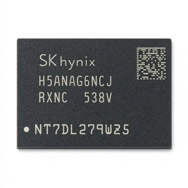
Quick Answers — What Is the H5ANAG6NCJR-XNC?
The H5ANAG6NCJR-XNC is a SK hynix 16Gb DDR4 SDRAM organized as 1G x 16. It operates at 3200 Mbps/pin from a 1.14 V to 1.26 V VDD/VDDQ supply and uses a surface-mount FBGA-96 package. The XAIPART database lists the component as active with 23,523 units in stock and a minimum order quantity of one. Pricing is tiered from $118.125 at one unit to $68.9063 at 1,000 units as of 2026-11-01.
This density, organization, and speed make the device suitable for systems that need 2 GB of volatile main memory per component without the x8 device-count required to populate a wider bus. Its verified features include auto self-refresh, auto precharge, asynchronous reset, data mask, dynamic on-chip termination, ZQ calibration, CRC, and write leveling. Review the H5ANAG6NCJR-XNC product page for current sourcing data and the manufacturer datasheet for implementation details.
Takeaway: Select the H5ANAG6NCJR-XNC when the design requires one 16Gb x16 DDR4 component, a 3200 Mbps/pin interface, and a 1.14 V to 1.26 V supply range.
Technical Guide — How Do You Design In the H5ANAG6NCJR-XNC?
Start with the system memory requirement rather than the headline data rate. The H5ANAG6NCJR-XNC provides 16 Gbit, or 2 GB, in one x16 organization. One device can therefore serve a 16-bit DDR4 memory channel, while two devices can provide 4 GB on a 32-bit DDR4 bus. This configuration is especially useful in soldered-down embedded modules where reducing device count simplifies routing and PCB area allocation.
| Parameter | Verified value | Design significance |
|---|---|---|
| Manufacturer | SK hynix | Use the H5ANAG6NCJR-XNC manufacturer documentation when qualifying the memory interface. |
| Memory type | DDR4 SDRAM | Requires a DDR4-compatible memory controller and DDR4 system-level power design. |
| Memory size | 16 Gbit | Provides 2 GB of volatile memory per component. |
| Organization | 1G x 16 | Supports a 16-bit data lane and uses a data mask function for x16 operation. |
| Data rate | 3200 Mbps/pin | Provides approximately 51.2 Gb/s of peak bandwidth per component at the full data rate. |
| Supply voltage range | 1.14 V to 1.26 V for VDD/VDDQ | Sets the required operating range for the memory power rails. |
| Interface | Parallel | Requires a compatible parallel DDR4 controller interface and matched routing. |
| Package | FBGA-96 | Supports compact, surface-mount PCB integration. |
| Mounting type | Surface mount | Requires an FBGA assembly process and a package-specific land pattern. |
| Packaging | Tray | Defines the supplied component packaging format. |
| RoHS status | Compliant | Supports lead-free assembly requirements subject to the applicable production process. |
The organization decision is more important than a small difference in headline speed. An x16 device reduces the number of components needed for a given data width, but it does not provide the byte-wide ECC arrangement associated with x8 DDR4 devices. Use the H5ANAG6NCJR-XNC for a 16-bit channel that does not require side-band or inline byte ECC. If the controller and system architecture require x8 devices for byte ECC, qualify an x8 part instead.
Power design must cover the full 1.14 V to 1.26 V VDD/VDDQ range. Do not assume that a nominal 1.2 V rail alone satisfies every operating condition. Use the manufacturer datasheet's voltage, current, and timing tables to set the regulator tolerance, power sequencing, and rail budgets for the final board. The verified product record confirms auto self-refresh, auto precharge, asynchronous reset, data mask, dynamic on-chip termination, ZQ calibration, CRC, and write leveling; those features support power management, data integrity, and signal-integrity functions in the target system.
| Verified function | Implementation role |
|---|---|
| Auto self-refresh | Supports retention during low-power operating states identified in the device documentation. |
| Auto precharge | Supports the device's automatic precharge operation. |
| Asynchronous reset | Provides an asynchronous reset function for system recovery. |
| Data mask | Supports masked data operation in the x16 organization. |
| Dynamic ODT | Provides dynamic on-chip termination. |
| ZQ calibration | Supports calibration of the device's output impedance. |
| CRC | Adds a data-integrity check function. |
| Write leveling | Supports training of write timing at the system interface. |
Plan the PCB layout around the FBGA-96 device and the controller's DDR4 routing requirements. Keep the memory close enough to the controller to support controlled trace lengths, preserve the VDDQ reference plane, and provide the routing topology expected by the memory controller. The component database identifies fly-by and point-to-point topologies as relevant implementation options, but it does not provide a board-specific length-matching table. Use the controller implementation guidance and the manufacturer package information to set the actual topology, escape routing, and per-byte matching limits.
Signal integrity does not stop at trace matching. Dynamic on-chip termination, ZQ calibration, CRC, and write leveling must all be supported by the selected controller and its training sequence. Include the -XNC operating condition in the controller's validated memory configuration. A controller operating at the supported voltage, timing, refresh, and training settings is more important than nominal bandwidth alone.
For industrial controllers, embedded modules, smart TVs, set-top boxes, and networking line cards, the component supplies 2 GB per package while limiting the number of devices needed on the memory bus. The database also identifies auto self-refresh for standby operation, asynchronous reset for recovery after a watchdog fault, and CRC for data-integrity checking. These functions support the target applications, but final qualification must still cover the controller, PCB stackup, operating environment, and production test process.
Assembly planning should account for the FBGA-96 format and tray packaging. Confirm that the assembly house has a qualified process for the device's ball pitch and package geometry. Use the approved package land pattern and assembly profile rather than inferring dimensions from the 96-ball count. Before releasing a production order, compare the incoming part markings, package drawing, speed-bin designation, and quantity against the purchase specification.
| Order quantity | Verified unit price as of 2026-11-01 |
|---|---|
| 1 or more | $118.125 |
| 10 or more | $85.3125 |
| 100 or more | $75.4688 |
| 500 or more | $72.1875 |
| 1,000 or more | $68.9063 |
The pricing table shows why quantity planning affects the component cost. The unit price falls from $118.125 at one unit to $68.9063 at 1,000 units as of 2026-11-01. Base the buy quantity on the verified demand, production schedule, and inventory policy rather than assuming the lowest tier applies to prototype orders.
Takeaway: Qualify the memory controller, voltage range, training sequence, FBGA-96 land pattern, and assembly process before committing the H5ANAG6NCJR-XNC to a PCB release.
Alternatives & Comparison — Which Drop-In Alternatives Are Verified?
The supplied alternatives dataset contains no populated component records with complete product_specs data. As a result, this guide does not present any alternative as a verified drop-in replacement. A valid drop-in comparison must establish more than the package name: density, organization, data rate, supply range, package, speed-bin behavior, and controller compatibility must all be matched or explicitly reviewed.
The comparison below therefore documents the verified H5ANAG6NCJR-XNC baseline and clearly identifies the absence of qualified alternative records. This approach prevents an x16 device from being mistaken for an x8 replacement or a different-density DDR4 part merely because both use FBGA packages.
| Parameter | H5ANAG6NCJR-XNC | Drop-in alternative status |
|---|---|---|
| Manufacturer | SK hynix | No populated alternative product_specs record supplied |
| Memory type | DDR4 SDRAM | No populated alternative product_specs record supplied |
| Memory size | 16 Gbit | No populated alternative product_specs record supplied |
| Organization | 1G x 16 | No populated alternative product_specs record supplied |
| Data rate | 3200 Mbps/pin | No populated alternative product_specs record supplied |
| Supply voltage range | 1.14 V to 1.26 V for VDD/VDDQ | No populated alternative product_specs record supplied |
| Interface | Parallel | No populated alternative product_specs record supplied |
| Package | FBGA-96 | No populated alternative product_specs record supplied |
| Mounting type | Surface mount | No populated alternative product_specs record supplied |
| Lifecycle status | Active | No populated alternative lifecycle record supplied |
When a candidate becomes available for review, compare it against this baseline rather than relying on the “DDR4-3200” label alone. An x8 part changes the bus organization and may change the ECC architecture. A lower-speed part may require controller training at a different setting. A larger-density part may change power, refresh, and loading requirements. A cross-brand device may use a different die revision and different qualification history. Only a completed parameter and controller review supports a drop-in claim.
The XAIPART component catalog can be used to monitor newly added alternatives, but the current article does not convert an unverified candidate into a recommendation. Buyers should also review related technical coverage through the XAIPART Blog before changing a qualified memory source.
Takeaway: Treat the H5ANAG6NCJR-XNC as the verified comparison baseline and do not approve a drop-in substitute until its complete product_specs and lifecycle records are available for review.
Industry Insight — What Does the Active Lifecycle and Stock Position Mean?
The XAIPART database classifies the H5ANAG6NCJR-XNC as active. That status supports continued design-in and sourcing activity, but it should not be treated as a forecast of future price, lead time, or production capacity. The available supply indicator is 23,523 units in stock, with a minimum order quantity of one. No date-specific allocation history, market-share figure, or manufacturer capacity forecast is included in the verified record.
| Supply and lifecycle indicator | Verified database status |
|---|---|
| Lifecycle status | Active |
| Stock | 23,523 units |
| Minimum order quantity | 1 |
| Packaging | Tray |
| RoHS status | Compliant |
The low MOQ is useful for prototypes, small builds, and replacement sourcing because engineers can order one unit without a large initial commitment. For production, the available stock quantity should be checked against the build plan rather than treated as a reservation. The database also supports alternate sourcing through the product page, but a second source is still a component-change candidate until its electrical, timing, package, and lifecycle data are verified.
Pricing remains sensitive to order volume. The verified tiers range from $118.125 for one unit to $68.9063 for 1,000 units as of 2026-11-01. Buyers should compare those breakpoints with forecast consumption and procurement lead time. A lower unit price does not necessarily reduce total sourcing cost if it requires more inventory than the program can consume.
The device's market position should be described conservatively: it is an active SK hynix DDR4 memory IC listed in XAIPART's Memory ICs category. The verified data does not establish vendor market share, unit shipment volume, or future supply allocation. Use the active status and current stock to support sourcing decisions, but request a production quote and availability confirmation for scheduled builds.
Takeaway: The part is currently active with 23,523 units listed and an MOQ of one, so prototypes can be sourced directly while production teams should still validate quantities against their build forecast.
Trends & Outlook — What Should Buyers Monitor?
The first design trend to monitor is continued demand for higher memory density without proportional increases in component count. The H5ANAG6NCJR-XNC combines 16 Gbit with a 1G x 16 organization, allowing a 32-bit DDR4 bus to reach 4 GB with two components. That configuration supports embedded computing modules, industrial controllers, smart TV and set-top box main memory, and networking line cards.
The second trend is bandwidth per package. At 3200 Mbps/pin, the x16 component provides approximately 51.2 Gb/s of peak bandwidth per device. Designs that move video frames, packet buffers, control data, or embedded operating-system workloads should evaluate whether one x16 device provides enough bandwidth or whether a wider bus with additional components is required.
The third consideration is power-constrained integration. The 1.14 V to 1.26 V VDD/VDDQ range, auto self-refresh, and dynamic on-chip termination give engineers defined tools for balancing memory performance with operating power. Buyers should verify the complete memory power budget, including controller-side and termination behavior, rather than estimating system power from the nominal supply voltage alone.
Signal integrity remains a decisive factor at 3200 Mbps/pin. Dynamic ODT, ZQ calibration, CRC, and write leveling are verified functions on this component, but their value depends on a compatible controller, correct training, controlled PCB routing, and a qualified manufacturing process. New platform designs should preserve the -XNC speed-bin configuration in the validated memory configuration rather than treating the component as a generic 16Gb DDR4 device.
Finally, monitor lifecycle and stock changes as closely as electrical specifications. The current active status, 23,523-unit stock position, MOQ of one, and tiered pricing as of 2026-11-01 provide a workable sourcing baseline. Recheck the H5ANAG6NCJR-XNC product record before each build because availability and quote freshness can change. Technical teams should also use the XAIPART article on bandwidth and sourcing questions as broader context, while keeping the component decision anchored to the verified DDR4 specifications.
Takeaway: Monitor density per package, 3200 Mbps/pin bandwidth, the 1.14 V to 1.26 V supply range, controller training, and lifecycle availability together; any one factor alone does not qualify a production design.
تبصرے
پہلا تبصرہ کرنے والے بنیں۔
🔐 براہ کرم سائن ان کریں تبصرہ شائع کرنے کے لیے۔
اکاؤنٹ نہیں ہے؟ سائن اپ کریں