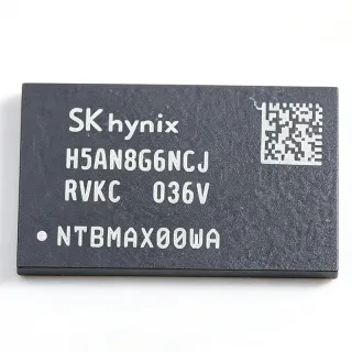
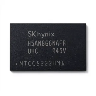
H5ANAG6NCJR-XNC - 16Gb DDR4-3200 SDRAM x16 | SK Hynix
MPN: H5ANAG6NCJR-XNC ✓ Active| Qty | Unit Price | Extended |
|---|---|---|
| 1 | $85.23 | $85.23 |
| 10 | $85.15 | $851.50 |
| 100 | $85.08 | $8,508.00 |
| 500 | $85 | $42,500.00 |
| 1,000 | $84.97 | $84,970.00 |
H5ANAG6NCJR-XNC Overview
DDR4 SDRAM (Double Data Rate 4 Synchronous Dynamic Random Access Memory) is the fourth generation of the DDR DRAM family, a class of volatile memory ICs that transfer data on both clock edges to achieve high bandwidth. In the memory hierarchy, DRAM sits between CPU caches and non-volatile storage such as NAND flash, serving as the primary working memory in computing systems. DDR4 doubled bank counts versus DDR3, lowered operating voltage from 1.5V to 1.2V, and added features such as bank grouping and a DBI (data bus inversion) option.
Key features of this device include auto self-refresh, auto precharge, asynchronous reset, data mask (DM) function for x16 operation, dynamic on-chip termination (ODT), ZQ calibration, CRC function, and write leveling - all of which improve signal integrity and simplify high-speed memory controller interfacing. The x16 organization suits systems that do not require dedicated ECC devices, allowing one chip per 16-bit data lane.
The -XNC speed bin supports 3200 Mbps/pin data rates at a CAS latency appropriate for DDR4-3200 operation, delivering roughly 51.2 Gb/s of peak bandwidth per component at full rate. The 96-ball FBGA surface-mount package keeps inductance low, which is essential at 3200 Mbps where trace-length matching, reference VDDQ planes, and on-die termination determine timing margin.
Typical applications include industrial controllers and embedded computing modules, networking equipment line cards, set-top boxes, smart TVs, and replacement sourcing for legacy DRAM DIMM/module designs. The 16Gb density is well suited to designs needing 2 GB or more per component without the complexity of ECC with x8 parts.
When designing with this part, keep fly-by or point-to-point topologies length-matched, verify the memory controller supports 16-bit data mask operation, and follow the JEDEC DDR4 power-ramp sequencing requirements for VDD, VDDQ, and VPP rails.
This page synthesizes distributor pricing, same-package drop-in alternatives, and practical design notes not found in the manufacturer datasheet, with data verified as of 2026-09-04.
Drop-in alternatives for H5ANAG6NCJR-XNC — same package, pin-to-pin compatible. Different-package parts requiring PCB rework are excluded.
Variants in this series
Same-series models that are drop-in compatible with H5ANAG6NCJR-XNC (same form factor and footprint) — differing in Package, Interface, Data Rate, Density, Memory Type.
Quick Comparison Tool — Select alternative parts for side-by-side comparison:
H5ANAG8NCJR-XNC
✅ Drop-In✓ In Stock
$65.625 / Unit
View Datasheet →H5ANAG6NBJR-VKC
✅ Drop-In✓ In Stock
$15 / Unit
View Datasheet →H5ANAG6NBJR-UHC
✅ Drop-In✓ In Stock
$8.09 / Unit
View Datasheet →H5ANAG6NBJR-RDC
✅ Drop-In✓ In Stock
$9.6 / Unit
View Datasheet →H5ANAG6NBJR-PBC
✅ Drop-In✓ In Stock
$6.45 / Unit
View Datasheet →H5ANAG8NCMR-VKC
✅ Drop-In✓ In Stock
$8.05 / Unit
View Datasheet →MT40A1G16TD-062E
✅ Drop-In✓ In Stock
$18.41 / Unit
View Datasheet →H5ANAG6NCJR-XNC Maximum Ratings & Electrical Characteristics
| Memory Type | DDR4 SDRAM |
| Memory Size | 16 Gbit |
| Memory Organization | 1G x 16 |
| Data Rate | 3200 Mbps/pin |
| Supply Voltage Range | 1.14 V to 1.26 V (VDD/VDDQ) |
| Interface | Parallel |
| Package | FBGA-96 |
| Mounting Type | Surface Mount |
| Auto Self-Refresh | Yes |
| Auto Precharge | Yes |
| Asynchronous Reset | Yes |
| Data Mask Function | Yes |
| Dynamic On-Chip Termination (ODT) | Yes |
| ZQ Calibration | Yes |
| CRC Function | Yes |
| Write Leveling | Yes |
| Packaging | Tray |
| RoHS Status | Compliant |
H5ANAG6NCJR-XNC fbga-96 Pin Configuration Guide
Pin configuration for H5ANAG6NCJR-XNC (fbga-96 package). This digital IC includes GPIO, communication interfaces (UART, SPI, I2C), and power pins. Refer to the manufacturer datasheet for alternate pin functions and configuration options. Essential for embedded system design and PCB layout.

No detailed pinout data available for H5ANAG6NCJR-XNC.
Refer to the datasheet for full pin configuration.
Typical Applications
H5ANAG6NCJR-XNC is suitable for 6 applications: Industrial Controllers and Automation, Embedded Computing Modules, Smart TV and Set-Top Box Main Memory, Networking Equipment Line Cards, Replacement Sourcing and Legacy Module Repair, Automotive-Adjacent Infotainment and Display Modules.
Industrial Controllers and Automation
Industrial PLCs, motion controllers, and edge automation gateways need dense volatile memory to buffer process data, run real-time operating systems, and log events. The H5ANAG6NCJR-XNC provides 2 GB per component in a single FBGA-96 footprint, and its 3200 Mbps/pin rate supplies roughly 51.2 Gb/s of peak bandwidth for deterministic control loops. Auto self-refresh keeps contents during machine standby, and the asynchronous reset function allows the host to recover the DRAM state machine after a watchdog fault without full power cycling. On-chip termination and ZQ calibration maintain signal integrity across the longer, impedance-tolerant traces typical of industrial PCBs.
Recommended
Embedded Computing Modules
SOMs and COM Express modules for networking appliances, medical instruments, and test equipment use soldered-down DRAM to avoid DIMM connectors and improve vibration immunity. The H5ANAG6NCJR-XNC's 16Gb x16 organization lets a module reach 4 GB with just two components on a single 32-bit DDR4 bus, halving BOM cost and board area versus eight 4Gb parts. Its 1.14V to 1.26V supply keeps module power within typical 5 W thermal budgets, while CRC and write leveling simplify high-speed routing on six-to-eight-layer stackups. Memory controller training tables should include the -XNC speed bin timings for reliable boot at full rate.
Recommended
Smart TV and Set-Top Box Main Memory
Broadcast and streaming SoCs with integrated DDR4 x16 controllers pair naturally with the H5ANAG6NCJR-XNC: the x16 data mask function matches the controller's 16-bit lane, and 16Gb density supports 4K video frame buffers, de-jitter buffers, and application memory on a single chip. The 3200 Mbps data rate provides bandwidth headroom for dual 4K30 decode plus UI compositing, while dynamic ODT reduces standby termination power in always-on consumer devices. The FBGA-96 package mounts directly under or beside the SoC, shortening the DQ/DQS nets and easing length matching in cost-driven two-to-four-layer consumer boards.
Recommended
Networking Equipment Line Cards
Access switches, routers, and PoE gateways use soldered DDR4 for packet buffers, route tables, and management-plane code. The H5ANAG6NCJR-XNC's high 3200 Mbps rate and low 1.2V-class rail help meet the bandwidth-versus-watt budget of fanless network hardware, and CRC support adds a hardware check on data integrity for control-plane structures. Auto precharge reduces controller command overhead in random-access buffer patterns typical of packet processing. Designs commonly place one or two components per management SoC, relying on ZQ calibration and write leveling to close timing across backplane-adjacent routing.
Recommended
Replacement Sourcing and Legacy Module Repair
The H5ANAG6NCJR-XNC is widely sourced as a replacement component for DDR4 DIMM/module production lines and board-level repairs where the original DRAM die is on allocation or end-of-life. Because the FBGA-96 x16 ball map follows the JEDEC DDR4 convention, reballing or direct BGA rework onto existing land patterns is feasible, and distributors including LCSC, WIN Source, Ampheo, and AIChipLink maintain stock. When replacing a failed die, verify the speed bin markings on the original package and match or exceed them; the -XNC 3200 bin covers most down-speed requirements at 2666 and 2400.
Recommended
Automotive-Adjacent Infotainment and Display Modules
Digital cockpit displays and non-safety infotainment SoCs increasingly specify DDR4 over LPDDR for bandwidth-per-dollar. The H5ANAG6NCJR-XNC supplies 2 GB in one FBGA-96 package, enough for dual HD display buffers plus navigation, and its auto self-refresh with self-refresh entry/exit supports the fast suspend/resume behavior drivers expect. Data mask simplifies partial-frame updates from the display pipeline. Note this commercial-grade part must be evaluated against the actual temperature profile of the cabin environment; for AEC-Q100-grade requirements, select a qualified automotive DRAM variant instead.
Recommended
Recommended Products Summary
Engineering reference data for H5ANAG6NCJR-XNC — comparison, design guidance, and compliance information.
Selection Guide
Comparison with Alternatives
| Parameter | This Product | H5ANAG8NCJR-XNC | H5ANAG6NBJR-VKC | MT40A1G16TD-062E |
|---|---|---|---|---|
| Brand | SK Hynix | SK Hynix | SK Hynix | Micron Technology |
| Package | FBGA-96 | FBGA-96 family | FBGA-96 - same | FBGA-96 - same JEDEC ball map |
| Memory Size | 16 Gbit | 16 Gbit | 16 Gbit | 16 Gbit |
| Organization | 1G x 16 | 512M x 8 | 1G x 16 | 1G x 16 |
| Data Rate | 3200 Mbps/pin | 3200 Mbps/pin | 2666 Mbps/pin | 3200 Mbps/pin class |
| Supply Voltage | 1.14 V - 1.26 V | 1.14 V - 1.26 V | 1.14 V - 1.26 V | 1.2 V class |
| Technology | DDR4 | DDR4 | DDR4 | DDR4 |
| Lifecycle Status | Active | Active | Active | Active |
Key Differentiators
- DDR4-3200 speed bin in x16 organization (vs H5ANAG6NBJR-VKC)
- x16 data mask simplifies 16-bit controller integration (vs H5ANAG8NCJR-XNC)
- Cross-brand second source availability (vs MT40A1G16TD-062E)
Design Notes
At 3200 Mbps/pin, DDR4 timing budgets are dominated by inter-symbol interference and ISI-driven eye closure on DQ/DQS nets. Use fly-by topology for address/command with per-byte lane length matching within +/-25 mils for the x16 data group, route over an unbroken VSS reference plane, and enable dynamic ODT with ZQ calibration (ZQ resistor 240 ohm +/-1%) as designed in SK Hynix reference layouts. Avoid stubs entirely - every via in the DQ path adds discontinuity at 1600 MHz fundamental data rate.
Estimated: with VDD = VDDQ = 1.2 V and standby current up to 0.074 A per the distributor spec, standby power is roughly 89 mW per chip; active power during streaming reads will be several times higher and must be budgeted from the datasheet IDD tables at your actual utilization. Decouple with a low-ESR bulk capacitor per rail plus one 0.1 uF ceramic per power ball group placed within 2 mm. Follow JEDEC DDR4 ramp-rate requirements for controlled VDD/VDDQ/VPP power-up sequencing to avoid latch-up during brown-out events.
Three frequent failures with x16 DDR4: (1) omitting the data mask (DM) connection - on x16 parts DM replaces the byte-wise TDQS scheme used on x8 parts, and leaving it floating corrupts partial writes; (2) running the memory controller speed tables above the -XNC bin capability or, conversely, under-training at 3200 when the PCB cannot support it - validate with margin testing at temperature extremes; (3) forgetting the asynchronous reset (RESET_n) tie-down during power ramp, which can leave the DRAM in an undefined ODT state and draw excess current at boot.
Place the H5ANAG6NCJR-XNC within 50 mm of the controller for point-to-point 16-bit designs, or follow the fly-by clock/CMD routing convention for multi-rank topologies. Keep the 240 ohm ZQ resistor on its own precision ground return with no switching signals nearby. Reference VDDQ planes must be solid under the data groups; splits force return-path detours that show up as eye shrink at 3200 Mbps. Include the FBGA-96 land pattern with NSMD pads and via-in-pad avoided within the ball field.
Compliance Information
RoHS compliance explicitly stated in LCSC product listing. REACH, lead-free, halogen-free, and conflict-minerals declarations not found in provided data - request certificate from SK Hynix.