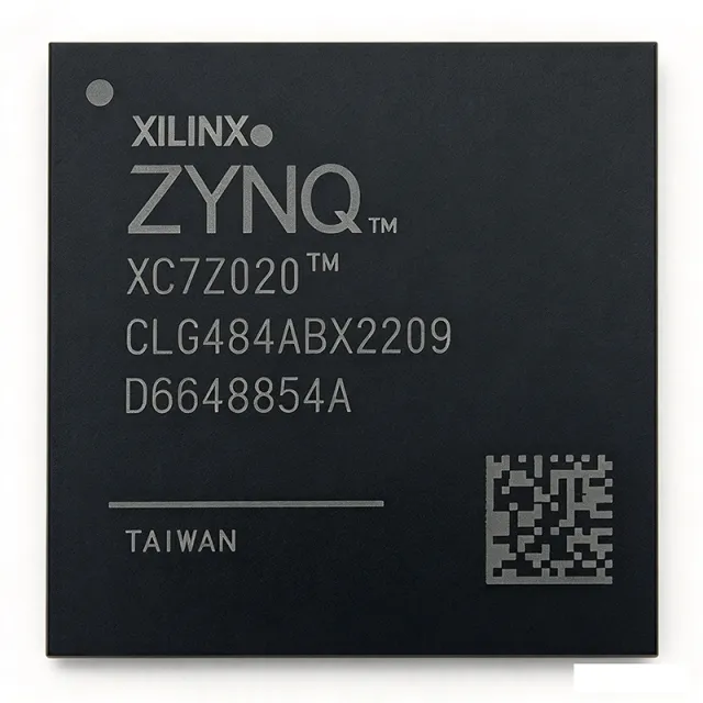
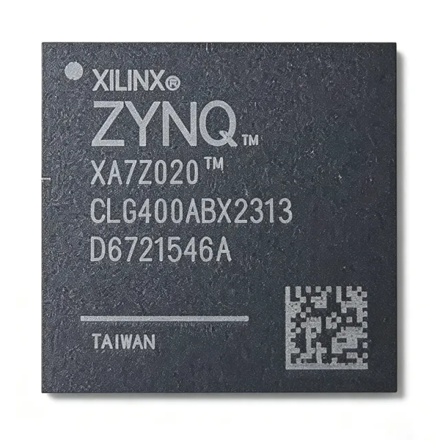
XC7Z020-1CLG400I
XC7Z020-1CLG400I - Dual-Core Cortex-A9 SoC FPGA | AMD
The AMD XC7Z020-1CLG400I is a programmable system-on-chip combining a dual-core Arm Cortex-A9 processor with an Artix-7 FPGA fabric, 85K logic cells, and a 667 MHz processor clock in a 400-CSPBGA package measuring 17 x 17 mm. The device also includes CoreSight debug and observation resources. This combination integrates hard-processor and programmable-logic functions on one package, making the XC7Z020 suitable for embedded control, data processing, industrial automation, communications, and test systems.
A Zynq-7000 SoC is a heterogeneous embedded computing device that combines an Arm Cortex-A9 application processing unit with an FPGA fabric. The processor executes operating-system and application software, while the programmable logic implements parallel data paths, custom interfaces, accelerators, and signal-processing functions. This product hierarchy places the XC7Z020 at the intersection of embedded processors, FPGA and CPLD devices, and application-specific programmable SoCs.
The principal device attributes include dual Arm Cortex-A9 processor cores, 85K FPGA logic cells, a stated 667 MHz Cortex-A9 operating frequency, CoreSight capabilities, and a 400-CSPBGA package. The integrated architecture allows software-controlled systems to place time-critical or highly parallel operations in FPGA logic while retaining conventional program flow in the processor subsystem. Pin-compatible ordering options within the CLG400 family can support different speed, temperature, or power configurations when the device qualification and operating requirements are compatible.
The processor-based portion provides an Arm-based execution environment for control software, networking stacks, and embedded applications. The FPGA portion provides programmable combinational and sequential logic alongside fixed I/O resources, allowing designers to implement custom peripherals, data acquisition paths, protocol accelerators, or high-throughput parallel processing. Because both domains share the package and system fabric, interconnect between software and programmable logic can be established according to the AMD Zynq architecture and supported interfaces.
Typical implementations include industrial programmable logic controllers, factory monitoring gateways, camera and image-processing modules, medical instrumentation, industrial networking equipment, and embedded test platforms. In these systems, the Cortex-A9 cores can manage protocols and supervisory functions while FPGA logic accelerates sampling, filtering, encoding, or interface handling. The CLG400 package is particularly relevant to dense embedded designs where a large pin count, compact 17 x 17 mm body, and mixed processor-logic implementation are required.
PCB implementation requires careful allocation of power, ground, high-speed memory, and configurable I/O resources. Follow the AMD package pinout files and XC7Z020 data sheet for the exact CLG400 ball assignments, recommended power sequencing, decoupling, and differential-pair routing. Confirm the selected board configuration, memory interface implementation, and peripheral assignments with the complete Vivado design before fabrication.
This product page combines the identifiable processor, FPGA, package, and sourcing characteristics of the XC7Z020-1CLG400I with package-focused alternatives, engineering design notes, and a parameter comparison intended to accelerate component selection and board-level planning.
RFQ
رابطہ