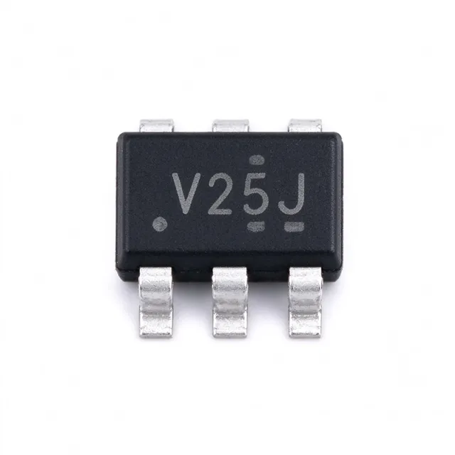
SN74CBTLV1G125DBVR - 3.3V Single FET Bus Switch SOT-23-5 | TI
MPN: SN74CBTLV1G125DBVR ✓ فعالSN74CBTLV1G125DBVR جائزہ
A bus switch (also called a FET switch or pass-gate switch) is a digital building block that replaces mechanical relays and discrete MOSFET switches in CMOS logic designs. The CBTLV family uses parallel n-channel and p-channel MOSFETs to provide a low-resistance bidirectional connection when enabled, achieving propagation delays under 0.25 ns. Bus switches sit within the logic-IC hierarchy as signal switches, above multiplexers and below general-purpose logic gates, and are essential for level shifting, signal multiplexing, and isolating subsystems on shared digital buses.
Key features include 5-ohm typ on-resistance (ron) measured at VCC = 3.3 V, rail-to-rail switching on data I/O ports, low quiescent current of 10 uA max, and 5.5 V tolerant I/O when VCC = 0 V thanks to the Ioff isolation. The SN74CBTLV1G125 is one of the smallest 1-channel bus switches available, making it ideal for space-constrained mobile and portable designs where a single high-speed line must be routed or isolated.
Architecturally, the device uses a parallel NMOS/PMOS pass gate controlled by a single OE-bar input. When OE-bar is low, both FETs turn on, creating a low-resistance channel between pin A (input) and pin Y (output); when OE-bar is high, the channel opens and the switch enters a high-impedance state. The Ioff circuitry prevents backfeeding through the switch when VCC is removed, eliminating parasitic current paths in partial-power-down or hot-swap scenarios.
Typical applications include USB type-C signal routing and protection, I2C/UART bus isolation in battery-powered devices, SD card muxing, GPIO expansion, and reset signal gating in microcontroller-based designs. The SOT-23-5 footprint makes the part convenient for hand-rework on prototype boards.
When designing with this device, place a 1 nF to 10 nF decoupling capacitor as close as possible to the VCC pin and observe ESD precautions when handling the small-outline package. Pull-up on OE-bar ensures defined behavior during power-up sequencing in microcontrollers with high-impedance control pins.
This page synthesizes distributor pricing, drop-in alternatives, and practical design notes not found in the manufacturer datasheet alone.
کے لیے ڈراپ اِن متبادل SN74CBTLV1G125DBVR — یکساں پیکیج، پن سے پن مطابقت پذیر۔ مختلف پیکیج والے پرزے جن کے لیے PCB دوبارہ کام درکار ہو، شامل نہیں ہیں۔
SN74LVC1G125DBVR
قیمت کے لیے رابطہ کریں
ڈیٹا شیٹ دیکھیں →SN74CBTLV1G125-Q1
📋 حوالہ جاتی متبادل (کیٹلاگ میں نہیں)
SN74CBTLV1G125DCKR
📋 حوالہ جاتی متبادل (کیٹلاگ میں نہیں)
SN74CBTD1G384DBVT
📋 حوالہ جاتی متبادل (کیٹلاگ میں نہیں)
74CBTLV1G125GW,125
📋 حوالہ جاتی متبادل (کیٹلاگ میں نہیں)
74CBTLV1G125DBVRE4
📋 حوالہ جاتی متبادل (کیٹلاگ میں نہیں)
SN74CBTLV1G125DBVR زیادہ سے زیادہ ریٹنگز اور برقی خصوصیات
| فنکشن | Bus Switch - 1:1 (SPST), 1-channel |
| ٹوپولوجی | 1 x SPST-NC |
| On-State Resistance (ron) | 5 ohm (typ) at VCC = 3.3 V |
| Supply Voltage (VCC) | 2.3 V to 3.6 V |
| اِن پٹ وولٹیج رینج | 0 V to 5.5 V tolerant |
| Quiescent Current (ICC) | 10 uA (max) |
| Output Enable (OE) Input | Active-low (OE-bar) |
| Ioff Partial-Power-Down | Supported |
| آپریٹنگ درجہ حرارت | -40C to +85C |
| پیکیج | SOT-23-5 (DBV) 2.9 x 1.6 mm |
| ماؤنٹنگ ٹائپ | Surface Mount |
| پن کی تعداد | 5 |
| MSL لیول | 1 (unlimited floor life) |
| RoHS اسٹیٹس | Compliant |
SN74CBTLV1G125DBVR پن کنفیگریشن
| پن 1 | OE-bar — Output enable, active-low; pulled high disables the switch |
| پن 2 | A — Switch input/output port A |
| پن 3 | GND — Ground reference |
| پن 4 | Y — Switch input/output port Y |
| پن 5 | VCC — Supply voltage, 2.3 V to 3.6 V |
عام استعمالات
SN74CBTLV1G125DBVR کے لیے موزوں ہے 6 ایپلیکیشنs: USB 2.0 Signal Routing & Muxing, I2C / UART Bus Isolation in Battery Devices, SD Card Signal Mux for Dual-Slot Readers, GPIO Expansion & Reset Gating, Level Shifting Between 3.3V and 5V Domains, Industrial Fieldbus & PLC I/O Routing.
USB 2.0 Signal Routing & Muxing
The SN74CBTLV1G125DBVR is ideal for USB 2.0 high-speed data-line routing in OTG and dual-role ports because its 5-ohm typical on-resistance adds minimal series loss and its sub-nanosecond propagation delay keeps the rise-time budget intact at 480 Mbps. Routed between a USB Type-C connector and an application processor, the part occupies only ~5 mm^2 of board area including the SOT-23-5 lands. Unlike a discrete MOSFET switch, the CBTLV requires no gate-driver bias network and supports 5 V short-to-bus protection on the connector side via Ioff. For USB 3.0 signaling above 5 Gbps, however, a higher-bandwidth alternative like the TS3A27518 is preferred.
تجویز کردہ
I2C / UART Bus Isolation in Battery Devices
The SN74CBTLV1G125DBVR cleanly inserts in series with SDA/SCL or TX/RX lines between a microcontroller and a peripheral that may be powered down independently. With VCC at 3.3 V and OE-bar driven high, the switch enters high-impedance and prevents leakage from the always-on rail into the sleeping subsystem. With OE-bar driven low, the 5-ohm channel is virtually transparent to I2C pull-up transitions, adding less than 50 ns of extra rise delay at 400 kHz Fast-mode. The Ioff isolation ensures that when the peripheral is at 0 V, no backfeed current can flow through the switch into the unpowered silicon, a critical feature for Li-ion battery designs with hot-swap docking.
تجویز کردہ
SD Card Signal Mux for Dual-Slot Readers
Where an embedded system needs to multiplex one SD host controller between two SD card sockets (for instance a removable-storage and an internal eMMC routing path), a single SN74CBTLV1G125DBVR can steer one signal line at the cost of ~5 mm^2. The part's passive pass-gate behavior means it does not need continuous clocking, and the Ioff feature keeps the unselected path inert during card insertion glitches. Designers should confirm the propagation skew against SD-card timing budgets; at 50 MHz SD clock the added delay is well under the 10 ns budget. For full 4-bit SD bus muxes the SN74CBT3253 is preferred, but the 1G125 remains the size-optimal solution for single-line steering.
تجویز کردہ
GPIO Expansion & Reset Gating
Microcontrollers frequently run out of GPIO pins when interfacing to multiple peripherals; the SN74CBTLV1G125DBVR lets one GPIO toggle or gate several downstream lines by steering through the pass-gate. It also serves as a reset-gating element, where OE-bar driven by the supervisor allows a clean discharged-reset propagation only when the supply rail is good. The part's low quiescent current of 10 uA max contributes negligible drain to battery-backed designs, and the 5.5 V tolerance on the switch path supports 1.8 V, 3.3 V, and 5 V mixed-rail systems. The SOT-23-5 package makes it easy to add reset gating even as a hand-soldered rework on legacy boards.
تجویز کردہ
Level Shifting Between 3.3V and 5V Domains
The SN74CBTLV1G125DBVR performs unidirectional level translation when VCC is tied to the lower-voltage rail (e.g., 3.3 V) and the data pins receive 5 V signals from a higher-voltage domain. The Ioff isolation clamps the body diode paths and prevents latch-up, allowing translation down to 0 V on VCC without forward-biasing internal junctions. For full bidirectional 3.3 V <-> 5 V level shifting on I2C-like buses, two CBTLV1G125 devices back-to-back is a common topology. Compared to dedicated level-translator ICs such as the TXS0108E, this approach is more flexible and consumes less than 50 uW quiescent power combined.
تجویز کردہ
Industrial Fieldbus & PLC I/O Routing
In factory-automation modules the SN74CBTLV1G125DBVR inserts in series with low-speed field-bus lines such as RS-485 direction-control paths or 24 V digital inputs that have been stepped down to 5 V logic. The part's wide -40C to +85C temperature range suits sealed control cabinets, and its 5.5 V tolerant I/O accepts inductive kickback from long cable runs. The SOT-23-5 footprint keeps the routing circuit compact on PLDs and modular I/O cards. For applications that demand AEC-Q100 or IEC 61508 SIL ratings, designers should select the SN74CBTLV1G125-Q1 or a dedicated functional-safety switch from TI's interface portfolio.
تجویز کردہ
تجویز کردہ پروڈکٹس کا خلاصہ
کے لیے انجینئرنگ ریفرنس ڈیٹا SN74CBTLV1G125DBVR — موازنہ، ڈیزائن رہنمائی، اور تعمیل کی معلومات۔
انتخاب کی گائیڈ
متبادلات کے ساتھ موازنہ
| پیرامیٹر | یہ پروڈکٹ | SN74CBTLV1G125-Q1 | SN74CBTLV1G125DCKR | SN74CBTD1G384DBVT | SN74LVC1G125DBVR | 74CBTLV1G125GW,125 |
|---|---|---|---|---|---|---|
| Brand | Texas Instruments | Texas Instruments | Texas Instruments | Texas Instruments | Texas Instruments | Nexperia |
| Package | SOT-23-5 (DBV) | SOT-23-5 (DBV) - same | SC-70-5 (DCK) - smaller but pin-compatible | SOT-23-5 - same | SOT-23-5 - same | SOT-23-5 - same |
| Function | 1-ch FET bus switch (SPST) | 1-ch FET bus switch (SPST) | 1-ch FET bus switch (SPST) | 1-ch level-translating switch | 1-ch non-inverting buffer/driver | 1-ch FET bus switch (SPST) |
| Operating Voltage | 2.3 V to 3.6 V | 2.3 V to 3.6 V | 2.3 V to 3.6 V | 2.3 V to 3.6 V | 1.65 V to 5.5 V | 2.3 V to 3.6 V |
| 5V Input Tolerant | Yes (with Ioff) | Yes (with Ioff) | Yes (with Ioff) | Yes (level translating) | Yes (with Ioff) | Yes |
| Automotive Grade | No | Yes (AEC-Q100 Grade 1) | No | No | No | No |
| Pin Count | 5 | 5 | 5 | 5 | 5 | 5 |
اہم امتیازی خصوصیات
- Smallest-footprint 3.3 V pass-gate with Ioff support (بمقابلہSN74CBTD1G384DBVT)
- Automotive-grade drop-in upgrade path (بمقابلہSN74CBTLV1G125-Q1)
- Cross-brand second source from Nexperia (بمقابلہ74CBTLV1G125GW,125)
ڈیزائن نوٹس
Place a 100 nF to 1 uF X5R/X7R decoupling capacitor within 2 mm of the VCC pin (pin 5) and connect its ground return directly to the device GND pin (pin 3) with the shortest possible trace. The SOT-23-5 thermal pad is not internally connected; use a copper pour on pin 3 and pin 5 only as needed for power routing. Keep high-speed signal traces on pin 2 (A) and pin 4 (Y) on the top layer with a continuous reference plane below to control characteristic impedance. Estimated trace impedance for a 50-ohm microstrip on standard FR-4 is consistent with a 0.4 mm-wide trace over a 4-layer stack at 0.2 mm dielectric.
Do not leave the OE-bar input floating - the line has internal pull-up behavior only in some CBTLV variants but never in the DBV family, so an un-driven OE-bar may float into the linear region and cause excess supply current. Drive OE-bar from a CMOS push-pull output or hold it low with a 100 kohm resistor to GND when unused. Do not exceed VCC = 3.6 V or the absolute maximum I/O voltage of 5.5 V. Designers migrating from the SN74CBTD1G125 must verify logic compatibility because the CBTD adds internal translation while the CBTLV is a passive pass-gate only.
Estimated: with a 5-ohm on-resistance plus a 15 pF load, the RC time constant is 75 ps and the 10-90 percent rise time at the output is roughly 170 ps - well within USB 2.0 Hi-Speed 480 Mbps eye-mask requirements. For multi-MHz signals keep the route length from pin A to pin Y under 25 mm and avoid right-angle bends; use 45-degree or curved traces to minimize discontinuity. If the switch sits near an antenna or RF trace, route GND under it to maintain a low-impedance return path and prevent common-mode noise injection through the parasitic body diode paths.
تعمیل کی معلومات
RoHS and REACH compliant per TI product page. Halogen-free per TI material declaration. Standard DBV is industrial-grade -40C to +85C; for AEC-Q100 select SN74CBTLV1G125-Q1



