VBUS054DD-HF4 - 4-Line USB ESD Protection TVS Array | Vishay
MPN: VBUS054DD-HF4 ✓ فعالVBUS054DD-HF4 جائزہ
A TVS (Transient Voltage Suppressor) diode array is a discrete semiconductor protection device that clamps fast transient overvoltages to safe levels, protecting downstream ICs from ESD, cable discharge, and surge events. TVS arrays belong to the broader protection-device hierarchy of diodes -> discrete semiconductors, and are commonly co-packaged as multi-channel arrays for high-speed serial interfaces where low capacitance is critical to avoid degrading signal integrity.
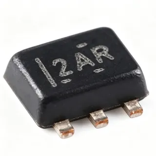
Key features include a working range of 5 V, snap-back clamping behavior, an operating temperature range of -40 °C to +125 °C, and a maximum peak pulse power dissipation tailored for USB 2.0 hot-plug and VBUS short-to-battery events. The LLP1010-5L package (1.0 mm × 1.0 mm) is roughly one-fourth the footprint of an SOT-23, enabling ultra-compact designs in mobile phones, wearables, and HDMI/USB-C accessories where board real estate is at a premium.
Architecturally, the VBUS054DD-HF4 integrates zener-based steering diodes that divert transient current away from protected data lines into the ground rail. The flow-through pinout routes D+/D- straight through the package while pin 5 serves as the common ground return, minimizing parasitic inductance and stub effects that would otherwise degrade USB 2.0 high-speed eye diagrams.
Typical applications include USB 2.0 / OTG port protection on smartphones and tablets, HDMI / DisplayPort interface ESD clamps, and 5 V VBUS rail transient protection on docking stations. The 0.8 pF typical capacitance makes it compatible with both USB 2.0 (480 Mbps) and low-speed USB 1.1 signaling.
When designing with this device, place it as close as possible to the external connector and ensure a low-impedance ground connection to pin 5. For USB 2.0 high-speed links, maintain 90 Ω differential impedance through the array and avoid routing high-current transient return paths underneath signal traces.
کے لیے ڈراپ اِن متبادل VBUS054DD-HF4 — یکساں پیکیج، پن سے پن مطابقت پذیر۔ مختلف پیکیج والے پرزے جن کے لیے PCB دوبارہ کام درکار ہو، شامل نہیں ہیں۔
VBUS054DD-HF4-GS08
✅ ڈراپ-اِن📋 حوالہ جاتی متبادل (کیٹلاگ میں نہیں)
VBUS054DD-HF4-GS18
✅ ڈراپ-اِن📋 حوالہ جاتی متبادل (کیٹلاگ میں نہیں)
VBUS054DD-HF4 تفصیلات
| Configuration | 4-line bus-port ESD protection |
| Working Voltage (Vrwm) | 5 V |
| Clamping Voltage | 19 V at 3 A (8/20 µs) |
| Peak Pulse Current (Ipp) | 3 A (8/20 µs) |
| ESD Air Discharge | ±15 kV per IEC 61000-4-2 |
| Line Capacitance | 0.8 pF typical |
| Breakdown Voltage (VBR) | 6.9 V to 8.7 V |
| Number of Protected Lines | 4 |
| Diode Type | Transient Voltage Suppressor (TVS), Zener steering |
| Arrangement | Common anode / steering-diode array |
| پیکیج | LLP1010-5L (1.0 mm × 1.0 mm) |
| ماؤنٹنگ ٹائپ | Surface Mount |
| آپریٹنگ درجہ حرارت | -40 °C to +125 °C |
| Marking Code | xC |
| RoHS اسٹیٹس | Compliant (HF4 suffix = Halogen-Free, RoHS-compliant) |
| Pinout | Flow-through (D1+, D2+, D1-, D2- on pins 1-4; GND on pin 5) |
VBUS054DD-HF4 پن کنفیگریشن
| پن 1 | D1+ — Data line 1 positive (USB D+ or HDMI TMDS0+) |
| پن 2 | D2+ — Data line 2 positive (USB VBUS or HDMI TMDS1+) |
| پن 3 | D1- — Data line 1 negative (USB D- or HDMI TMDS0-) |
| پن 4 | D2- — Data line 2 negative (HDMI TMDS1-) |
| پن 5 | GND — Common ground return for all four protected lines; tie to chassis ground with low-impedance path |
عام استعمالات
VBUS054DD-HF4 کے لیے موزوں ہے 6 ایپلیکیشنs: USB 2.0 Type-A Port ESD Protection, Smartphone / Mobile Device Charging Port, HDMI / DisplayPort Interface ESD Clamp, Docking Station / Hub Downstream Port, Automotive Infotainment USB Port, Wearable / Fitness Tracker Side Port.
USB 2.0 Type-A Port ESD Protection
The VBUS054DD-HF4 protects two USB 2.0 high-speed data lines (D+/D-) and the 5 V VBUS rail on a type-A connector. With 0.8 pF typical line capacitance the array adds <1 dB insertion loss at 240 MHz, preserving the USB 2.0 high-speed eye mask. The 19 V clamp voltage and ±15 kV air-discharge rating handle cable-discharge events that occur when a charged cable is plugged into an unpowered host. Place the array within 3 mm of the connector body and tie pin 5 (GND) to the chassis ground plane through 4 vias to maximize transient energy dissipation.
تجویز کردہ
Smartphone / Mobile Device Charging Port
Smartphone micro-USB / USB-C connectors experience daily mechanical wear and ESD events from human contact. The VBUS054DD-HF4's ultra-compact 1.0 mm × 1.0 mm LLP1010-5L footprint saves ~70% board area versus SOT-23 alternatives, a critical advantage in compact phones. The -HF4 halogen-free, RoHS-compliant finish meets Apple and Samsung green-material requirements. Its 19 V clamp tolerates VBUS inductive kickback from in-rush currents during hot-plug charging events, preventing downstream USB controller damage.
تجویز کردہ
HDMI / DisplayPort Interface ESD Clamp
HDMI and DisplayPort TMDS pairs (4 high-speed differential lines per connector) require sub-1 pF capacitance to maintain the 3.4 Gbps / 5.4 Gbps link signal integrity. The VBUS054DD-HF4's 4-line array protects exactly one TMDS pair plus the +5 V supply and hot-plug-detect pin. Its 0.8 pF typical capacitance introduces minimal jitter, while ±15 kV air-discharge rating complies with HDMI 1.4 ESD stress tests. Place the array immediately adjacent to the HDMI connector body to minimize loop area on the discharge path.
تجویز کردہ
Docking Station / Hub Downstream Port
Docking stations typically expose 4-8 downstream USB ports that each need independent ESD protection. The VBUS054DD-HF4's small footprint allows one TVS array per port without crowding the PCB. Its 19 V clamp and 3 A peak pulse current handle the energy from a VBUS short-to-battery fault on an attached device, protecting the upstream hub controller (such as USB2513B-AEZC). Tie pin 5 to the chassis ground plane to bleed chassis-coupled transients.
تجویز کردہ
Automotive Infotainment USB Port
In-vehicle USB ports experience harsher ESD events from occupant contact plus ISO 7637-2 transient disturbances on the 12 V supply rail. The VBUS054DD-HF4's -40 °C to +125 °C operating range covers the AEC-Q100 automotive temperature window, and its 19 V clamp tolerates the load-dump transients typical of automotive power nets. Pair the array with a bulk TVS such as the SMBJ24A on the VBUS rail for two-stage protection.
تجویز کردہ
Wearable / Fitness Tracker Side Port
Fitness bands and smartwatches expose charging pins that, while not true USB, mimic the D+/D-/VBUS topology and require the same ±15 kV ESD robustness. The VBUS054DD-HF4's 1 mm × 1 mm footprint fits within a 6 mm × 6 mm PCB corner near the pogo-pin landing pad. Its 19 V clamp tolerates the inductive kick from the magnetic charging-cable disconnect event, protecting the battery-management IC. Choose the -HF4 halogen-free finish to comply with medical-adjacent wearable material standards.
تجویز کردہ
تجویز کردہ پروڈکٹس کا خلاصہ
کے لیے انجینئرنگ ریفرنس ڈیٹا VBUS054DD-HF4 — موازنہ، ڈیزائن رہنمائی، اور تعمیل کی معلومات۔
انتخاب کی گائیڈ
متبادلات کے ساتھ موازنہ
| پیرامیٹر | یہ پروڈکٹ | VBUS054DD-HF4-GS08 | VBUS054DD-HF4-GS18 | USBLC6-2SC6 | RClamp0521P |
|---|---|---|---|---|---|
| Brand | Vishay Intertechnology | Vishay Intertechnology | Vishay Intertechnology | STMicroelectronics | Semtech |
| Package | LLP1010-5L (1.0 × 1.0 mm) | LLP1010-5L - same | LLP1010-5L - same | SOT-23-6 - different (not pin-compatible) | SLP1006P2 - different (not pin-compatible) |
| Working Voltage (Vrwm) | 5 V | 5 V | 5 V | 5 V | 5 V |
| Clamping Voltage | 19 V at 3 A | 19 V at 3 A | 19 V at 3 A | 17 V at 5 A (tighter clamp) | 13 V at 1 A (tighter clamp) |
| Peak Pulse Current (8/20 µs) | 3 A | 3 A | 3 A | 5 A (higher rating) | 1 A (lower rating) |
| Line Capacitance | 0.8 pF typical | 0.8 pF | 0.8 pF | 1 pF (slightly higher) | 0.5 pF (lower) |
| Number of Protected Lines | 4 | 4 | 4 | 4 (2 data + VBUS + ID) | 1 (single line) |
| RoHS / Halogen-Free | Yes (HF4 suffix) | Yes | Yes | Yes (ECOPACK) | Yes |
اہم امتیازی خصوصیات
- Ultra-compact 1.0 × 1.0 mm LLP1010-5L footprint (بمقابلہUSBLC6-2SC6 (SOT-23-6))
- Flow-through pinout matches D+/D-/VBUS routing (بمقابلہUSBLC6-2SC6 (SOT-23-6))
- Halogen-free, RoHS-compliant -HF4 finish (بمقابلہOlder Vishay VBUS054DD variants without -HF4 suffix)
ڈیزائن نوٹس
Place the VBUS054DD-HF4 within 3 mm of the USB or HDMI connector body to minimize the transient discharge loop. The flow-through pinout (pins 1-4 carry D+/D-/VBUS signals; pin 5 is GND) requires that pin 5 be tied to the chassis ground plane through a minimum of 4 vias to provide a low-impedance return path for ESD current. Avoid routing high-current transient return paths underneath the protected signal traces to prevent coupling.
For USB 2.0 high-speed (480 Mbps) operation, maintain 90 Ω differential impedance through the VBUS054DD-HF4 footprint. The 0.8 pF typical capacitance introduces <1 dB insertion loss at 240 MHz, but PCB stub effects from improper pin 1/2/3/4 fanout can dominate signal degradation. Use a symmetrical pinout with matched trace lengths on D+ and D- and avoid via transitions within 5 mm of the array.
Estimated: under an 8/20 µs 3 A peak pulse, instantaneous power dissipation reaches 57 W in the VBUS054DD-HF4. While the pulse duration is short, repeated stress events (e.g., a hot-plug arc every few minutes in a test environment) can raise junction temperature. Ensure at least 10 mm² of 1 oz copper under the LLP1010-5L thermal pad for heat spreading, and consider the SMBJ24A on the VBUS rail as a coarser first-stage clamp to reduce stress on this part.
Do not use the VBUS054DD-HF4 to protect CC/SBU lines on USB Type-C ports without verifying that the 19 V clamp voltage is within the CC pin's 5 V tolerant specification - the 19 V clamp may damage the CC logic. For USB Type-C, use a dedicated CC protection part such as the TPD4E05U06 or ESD8004 instead. Also note that the -HF4 suffix indicates halogen-free finish; if a non-halogen-free version is required, the bare VBUS054DD-HF4 (without -HF4) is no longer widely stocked.
تعمیل کی معلومات
The -HF4 suffix indicates Halogen-Free and RoHS-compliant finish. Not AEC-Q100 qualified - consult Vishay's automotive-grade TVS arrays for AEC-Q100 requirements.