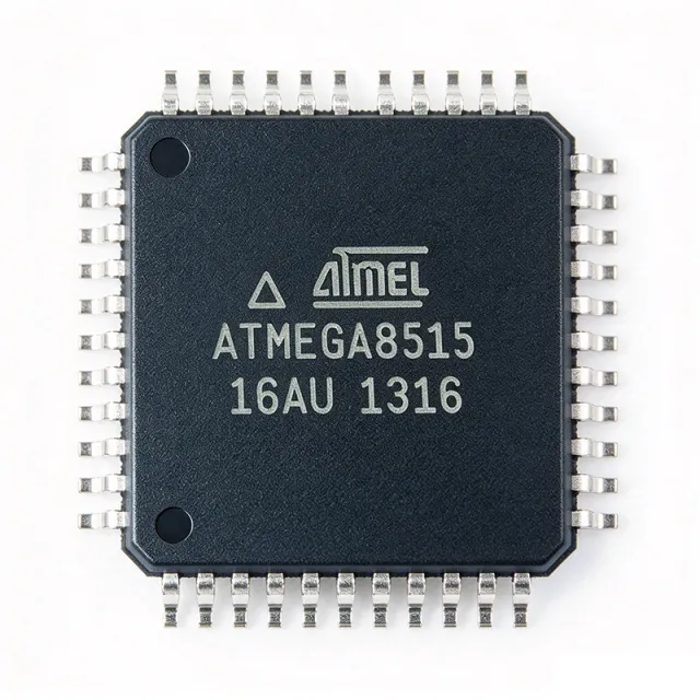
Quick Answers — What Is the ATMEGA8515-16AU?
The ATMEGA8515-16AU is an active, 8-bit AVR enhanced RISC microcontroller from Microchip Technology. It runs at up to 16 MHz and provides 16 MIPS of throughput, with 8 KB of in-system programmable Flash, 512 B of internal SRAM, 512 B of EEPROM, and an external SRAM interface supporting up to 64 KB. The device includes 35 programmable I/O lines, two 8-bit timers plus one 16-bit timer, USART, SPI, JTAG, an analog comparator, and a watchdog timer with an on-chip oscillator. It operates from 4.5 V to 5.5 V and comes in a lead-free 44-TQFP surface-mount package measuring 10 x 10 mm. Current availability is 16,000 units with an MOQ of one. Verified pricing starts at $4.37 for one unit and falls to $2.85 at 1,000 units, as of 2026-11-01. See the ATMEGA8515-16AU product page for current sourcing data.
Takeaway: Select the ATMEGA8515-16AU when a design needs deterministic 8-bit control, a 16 MHz clock, parallel external-memory support, and a lead-free 44-TQFP package rather than a larger-memory or lower-voltage MCU.
Technical Guide — How Do You Select and Design In the ATMEGA8515-16AU?
Begin with the memory and interface requirements. The ATMEGA8515-16AU provides 8 KB of Flash, 512 B of internal SRAM, and 512 B of EEPROM. That is enough for compact control firmware, state machines, communication handling, and modest data buffers. Its external SRAM interface is the defining feature: it can support up to 64 KB of off-chip SRAM when a design needs substantially more working memory than the internal 512 B can provide. Because that interface occupies Port A, Port C, and associated control pins, verify the board-level memory requirements before committing the pin budget.
The following table summarizes the verified design constraints most likely to determine whether the device fits.
| Parameter | Verified value | Design significance |
|---|---|---|
| Architecture and maximum frequency | 8-bit AVR enhanced RISC; 16 MHz | Supports 16 MIPS of instruction throughput at the maximum clock. |
| Program memory | 8 KB Flash, organized as 4K x 16 | Firmware capacity requires explicit budgeting for code, constants, and boot functions. |
| Internal data memory | 512 B SRAM | Limits simultaneous buffering and application-state capacity. |
| External SRAM support | Up to 64 KB | Provides a path to larger buffers, frame buffers, or protocol state tables. |
| EEPROM | 512 B | Supports nonvolatile configuration, settings, or fault data subject to firmware wear management. |
| I/O | 35 programmable lines | Supports keys, indicators, sensors, relays, and other digital interfaces. |
| Timers | Two 8-bit and one 16-bit | The 16-bit timer supports timebase, input-capture, and compare-based control functions. |
| Serial interfaces | USART, SPI, JTAG | Provides host communication, peripheral connectivity, and on-chip debug access. |
| Supply range | 4.5 V to 5.5 V | The design must remain within the verified operating range. |
| Package | 44-TQFP, 10 x 10 mm | Requires a surface-mount land pattern and assembly process designed for this package. |
| Temperature range | -40 C to +85 C | Covers the stated industrial operating range. |
Takeaway: Approve this MCU when 8 KB of code, 512 B of internal RAM, and 35 I/O lines meet the base design, and add external SRAM only when its board and firmware costs are justified.
How does the power design affect operation?
Connect the supply within the verified 4.5 V to 5.5 V VCC range. The recommended design practice for this device is to decouple AVCC with 100 nF and 10 µF and to keep the external-memory traces short. Although the MCU does not include an ADC in the verified specification set, maintaining clean analog supply and ground connections reduces coupling into adjacent signals and preserves the option to use the analog comparator in a future revision.
Use a 10 kΩ pull-up from RESET to VCC and fit a 100 nF capacitor from RESET to ground to improve reset noise immunity. The reset signal is active low on pin 9. Treat the reset network as part of the power and programming architecture rather than as an optional board detail, especially in industrial, appliance, or building-control products exposed to electrically noisy environments.
How should the external SRAM interface be routed?
Ports A and C carry the external-memory address and data functions, while ALE provides the address-latch function on pin 29. PD5 and PD6 provide the external-memory write and read strobes. Keep the memory bus short and route it as a controlled interface; the external SRAM path can operate at 16 MHz without providing the margin that slower, lower-frequency systems would offer. Follow the official datasheet for electrical characteristics, package details, and the complete pin assignment when laying out the memory bus.
The verified 64 KB external-memory capability is 128 times the internal 512 B SRAM capacity. This ratio shows why the interface matters in data-logging, display-buffer, or state-table applications, but it does not mean firmware can treat external and internal memory as interchangeable. Address mapping, access timing, and allocation remain design tasks.
Use the official ATmega8515 datasheet as the source for electrical limits, programming information, and the complete package pinout.
How do timers and serial interfaces support a control design?
The two 8-bit timers and one 16-bit timer provide separate resources for short timing intervals, longer timing intervals, input capture, and compare outputs. The 16-bit timer is the relevant resource for motor, valve, lighting, or other time-dependent control loops that need more resolution than an 8-bit timer provides. The verified pin list includes OC1A on pin 36, OC1B on pin 35, and ICP on pin 39.
Use USART for point-to-point host or field-bus transceiver links and SPI for higher-pin-count peripherals or external devices. JTAG provides a hardware debug path. For production firmware, select the programming and debug route early because the programming signals, reset behavior, and board-level connectors affect layout.
Six sleep modes are identified in the verified feature set, and the watchdog timer includes an on-chip oscillator. These resources support low-duty-cycle nodes and recovery from firmware hangs, but no verified numerical sleep-current or watchdog-timeout figures are provided in the supplied data. Use the manufacturer documentation for those limits before making a power-budget or safety-timing commitment.
What application patterns fit the verified feature set?
Industrial control and building-automation designs benefit from the 16 MHz clock, 35 I/O lines, 16-bit timer, and USART. Appliance controllers can use the timers for heating, motor, relay, or solenoid timing while retaining settings in EEPROM. Sensor interface nodes can combine digital inputs, the analog comparator, USART or SPI aggregation, and the watchdog timer. HMI front panels can use the I/O and SPI resources for keypads, displays, indicators, and encoders, although the internal SRAM requires disciplined buffer sizing.
Arduino-style firmware development is also possible through community packages named in the verified application data, while JTAG remains available for production-grade debugging. The absence of a verified ADC specification means sensor designs requiring direct multi-channel analog conversion should not treat the comparator as an ADC replacement without a separately verified signal-conditioning and conversion design.
Takeaway: Build the power, reset, and external-memory layout first, then allocate timer and serial resources around the control task rather than adding peripherals after the firmware and pin budget are fixed.
Alternatives & Comparison — Which Drop-In Alternatives Are Available?
The verified alternatives data identifies one candidate in the same family: the AT90S8515-16AU. It shares the 44-TQFP footprint and AVR RISC core and retains 8 KB of Flash. The key distinction is peripheral capability: the AT90S8515-16AU lacks the ATMEGA8515-16AU's analog comparator and lacks some of its modern watchdog-related capabilities. A shared footprint and core therefore do not, by themselves, prove that firmware and peripheral behavior are interchangeable.
| Parameter | ATMEGA8515-16AU | AT90S8515-16AU | Selection consequence |
|---|---|---|---|
| Package | 44-TQFP | 44-TQFP | The alternatives data identifies the same footprint. |
| Core | AVR RISC, 8-bit | AVR RISC | Both use the AVR RISC family. |
| Flash memory | 8 KB | 8 KB | Program-memory capacity is unchanged in the supplied comparison data. |
| Analog comparator | Yes | Lacks the modern analog comparator feature identified in the alternatives data | Review any comparator-dependent firmware and signal path. |
| Watchdog capabilities | Watchdog timer with on-chip oscillator | Lacks some modern watchdog modes identified in the alternatives data | Confirm recovery behavior and timeout implementation before substitution. |
Do not select the AT90S8515-16AU solely because the PCB land pattern matches. Check every used peripheral, reset behavior, timer feature, firmware register definition, and application timing requirement. The safer use case is an intentional migration with a board and firmware review, not an unverified drop-in claim.
The separately verified purchasing FAQ identifies the ATMEGA8515-16JU as the closest SMD ordering option because it uses the same 44-TQFP footprint and shares the 16 MHz speed grade, Flash size, and pinout according to the supplied database answer. The ATMEGA8515-16PU is not a direct physical substitute because it uses a 40-pin PDIP package rather than the 44-TQFP package on the AU device.
Package choice remains an assembly decision. Use the AU for new automated SMD production and the PU only when the board and assembly process require through-hole DIP. Neither package change should be treated as permission to alter firmware without checking the complete device-specific pin and peripheral differences.
Takeaway: Treat the AT90S8515-16AU as a qualified migration candidate rather than an automatic drop-in, and verify firmware, peripheral, and timing differences before releasing a substitution.
Industry Insight — What Does Lifecycle and Supply Data Say About Availability?
The ATMEGA8515-16AU is listed as active in the XAIPART product database. This status indicates that the part remains available for current design and sourcing activity; it does not by itself establish long-term availability, uninterrupted production, or a formal lifecycle-duration commitment.
Current stock is 16,000 units with an MOQ of one. The verified pricing structure is $4.37 at quantities of one or more, $4.05 at 10 or more, $3.62 at 100 or more, $3.20 at 500 or more, and $2.85 at 1,000 or more, as of 2026-11-01. The $2.85 base price also corresponds to the 1,000-unit tier in the verified pricing data.
| Quantity threshold | Verified unit price | Freshness |
|---|---|---|
| 1 or more | $4.37 | As of 2026-11-01 |
| 10 or more | $4.05 | As of 2026-11-01 |
| 100 or more | $3.62 | As of 2026-11-01 |
| 500 or more | $3.20 | As of 2026-11-01 |
| 1,000 or more | $2.85 | As of 2026-11-01 |
The active lifecycle status, one-unit MOQ, and current inventory support prototype work, small builds, and production evaluation without waiting for a minimum assembly quantity. However, a point-in-time stock figure is not a guarantee against allocation, inventory cycling, or later demand changes. Buyers should use the XAIPART component catalog to check current stock when releasing each order and request a supply confirmation for scheduled production.
No market-share, competitor-volume, or multi-year production forecast is included in the supplied lifecycle and stock data. The defensible sourcing conclusion is therefore limited to the verified active status, 16,000-unit stock position, MOQ, and quantity pricing.
Takeaway: The part is currently active and well stocked, but schedule-critical programs should confirm allocation and lead time against each planned production run instead of relying on the present inventory snapshot.
Trends & Outlook — What Should Buyers Watch?
The most important trend for this MCU is not raw clock speed but the value of its mixed resource set. The ATMEGA8515-16AU combines a 16 MHz core, 16 MIPS throughput, 35 I/O lines, three timers, USART, SPI, and JTAG in a 10 x 10 mm 44-TQFP package. For industrial-control, appliance, building-automation, and legacy parallel-memory products, that combination can reduce the need for external I/O expansion and support both control and communications functions in one device.
Watch the 8 KB Flash and 512 B SRAM constraints in new firmware. More elaborate communications stacks, display buffering, or data-logging functions can consume memory quickly, while the external SRAM interface adds board complexity and consumes multiplexed pins. A design that starts with 8 KB and later expects larger runtime buffers should evaluate external memory early, using the XAIPART engineering resources to plan the hardware and firmware allocation together.
Also watch the distinction between supported hardware and ecosystem assumptions. USART and SPI make external transceivers and peripherals practical, and community firmware packages can simplify development. JTAG remains an advantage for production debugging. By contrast, the verified specification list does not include an ADC, so projects with direct analog measurement requirements should compare the analog comparator and external signal path against an MCU with a verified ADC.
Supply strategy should reflect the part's active status and current price tiers. Consolidating a forecast across the 100-, 500-, and 1,000-unit thresholds can lower unit cost, but inventory should follow the actual demand plan because the current 16,000-unit stock position can change. For legacy systems, the AT90S8515-16AU may provide a footprint-compatible migration path, but its missing modern peripheral features make firmware-level qualification essential.
For new connected products, compare the ATMEGA8515-16AU with controllers that provide more memory, lower-voltage operation, or broader modern peripherals when those requirements exceed the 8515's verified limits. For compact standalone controllers, however, the 5 V operating range, 35 I/O lines, timer set, and external-memory option can preserve a practical design without unnecessary expansion.
Takeaway: Buyers should watch memory headroom, analog-measurement requirements, external-SRAM implementation cost, and inventory freshness; these constraints determine whether the active ATMEGA8515-16AU remains the most economical choice as the design evolves.
Bình luận
Trở thành người đầu tiên bình luận.
🔐 Vui lòng đăng nhập để đăng một bình luận.
Bạn không có tài khoản? Đăng ký