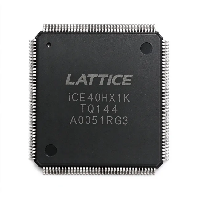
What is the ICE40HX4K-TQ144, and what specifications are verified?
The ICE40HX4K-TQ144 is a Lattice Semiconductor ultra-low-power FPGA in the iCE40 HX family. Verified specifications include 3,520 logic cells, 81,920 bits of configuration memory, 107 I/Os, a 1.2 V core supply, a 40 nm process, and a 144-pin TQFP surface-mount package. The database records the device as active and lists 19,500 units in stock with an MOQ of 1. Its verified base price is $10.6641 as of 2026-11-01. These figures make the part relevant to compact control, communications, data-acquisition, instrumentation, prototyping, and industrial digital-logic designs that require programmable parallel logic rather than a fixed-function digital IC.
Capacity is only the first selection point. Before committing the device to a PCB, confirm the exact package drawing, electrical limits, timing, temperature grade, supported I/O standards, configuration method, and power behavior in the applicable Lattice Semiconductor documentation. The supplied data identifies the package as 144-pin TQFP but also notes 144-LQFP terminology in distributor results, so engineers should treat that package discrepancy as a mandatory footprint check rather than assume either drawing applies.
Buyer takeaway: The ICE40HX4K-TQ144 combines verified 3,520-cell capacity with 107 I/Os and a 1.2 V core supply, while the active lifecycle status and listed inventory support further sourcing review.
How do you select and design in the ICE40HX4K-TQ144?
Start the selection with the logic and connectivity budget rather than the family label. The verified record gives designers 3,520 logic cells, 81,920 bits of configuration memory, and 107 I/Os. These resources fit moderate designs that combine state machines, parallel data paths, interface control, and multiple external signals. They do not establish the performance of a specific interface. Do not infer supported I/O standards, maximum clock frequency, RAM capacity, timing margins, or power consumption from the family description; the exact device documentation must support each of those decisions.
1. Match the design to the verified logic capacity
Use 3,520 logic cells as the available implementation capacity for control logic, framing, filtering, protocol conversion, acquisition pipelines, or sequencing. Actual utilization depends on routing, clocking, memory, and I/O requirements, so a design that uses several complex parallel paths may consume more resources than a simple set of counters and state machines. Compile the intended design with the Lattice toolchain instead of translating a logic-cell count directly into a guaranteed channel count or throughput.
The 81,920-bit configuration memory identifies the configuration capacity verified for this part. Treat it as a device-level record, not as user-accessible data memory. The supplied specifications do not define a separate RAM architecture, block-RAM quantity, or embedded-memory interface. Designs that require an internal data buffer must confirm the available memory resources in the exact device documentation and toolchain reports.
2. Budget the 107 external I/Os
The 107 I/Os provide connectivity for sensors, buses, status signals, configuration or debug connections, displays, actuators, and other board-level interfaces. Build an I/O inventory that separates data, control, clock, and status signals. Then verify each assigned signal against the manufacturer pin table and the electrical limits for the selected I/O standard.
| Verified selection parameter | ICE40HX4K-TQ144 value | Design implication |
|---|---|---|
| Logic cells | 3,520 cells | Plan implementation with compilation results rather than a cell-count estimate alone. |
| Configuration memory | 81,920 bits | Confirm the configuration workflow and image size in the toolchain. |
| I/O count | 107 I/Os | Reserve enough pins for external data, control, clocking, and programming functions. |
| Core supply voltage | 1.2 V | Design the core rail around the verified nominal requirement and confirm tolerance, current, and sequencing in the electrical documentation. |
| Package | 144-pin TQFP | Verify the mechanical drawing and land pattern before PCB release. |
| Process technology | 40 nm | Use the documented device data for final electrical and design decisions. |
3. Design the 1.2 V core rail and external interfaces
The verified core supply requirement is 1.2 V. That value makes the part consistent with low-power programmable logic, but it is not a complete power specification. The supplied data does not state core-current limits, quiescent current, active current, voltage tolerances, rail sequencing, or the supported I/O voltage range. Do not calculate a power budget from the nominal voltage alone. Obtain those values from the exact datasheet, then select the regulator, decoupling, and level-shifting strategy around the resulting current and voltage constraints.
For mixed-voltage systems, separate the core rail from external signal domains. Confirm each external pin's supported I/O standard and voltage range before connecting a sensor, processor, transceiver, or display. The 107-I/O count indicates available connectivity, not blanket compatibility with every voltage or interface standard.
4. Verify configuration, clocking, and programming access
The configuration interface is not specified in the supplied record, so do not assume a connector, serial protocol, or pin assignment. Use the manufacturer configuration workflow and the approved device support files to determine programming pins, configuration behavior, and board-level implementation. The FAQ source material also directs engineers to the manufacturer PDF for configuration and pin verification.
Clock requirements need the same treatment. No maximum operating frequency or speed grade appears in the verified specifications. Create the design with explicit clock constraints, then inspect timing reports using the device and toolchain settings authorized for this exact part. Do not substitute a family-level timing assumption for a device-level result.
5. Confirm the footprint and pin assignment
The verified package record is 144-pin TQFP with surface-mount mounting. That is useful for assembly planning, but it is not a substitute for a land pattern. The source material explicitly warns that distributor snippets alternate between 144-pin TQFP and 144-LQFP terminology. Download the applicable Lattice package drawing, verify pin numbering, body dimensions, lead geometry, and any thermal or exposed-pad details, and reconcile the mechanical drawing with the chosen distributor part number before releasing Gerber files.
Pin-level release should include a second review of power, ground, configuration, clock, and user-I/O assignments. The verified data does not include individual pin names, so no pin map is reproduced in this guide. The ICE40HX4K-TQ144 datasheet remains the required starting point for the complete pin and electrical review.
6. Validate the application instead of relying on a use-case label
Typical supported design directions include custom communications interfaces, low-power sensor aggregation, programmable data acquisition, education and prototyping, instrument control, and industrial digital control. Use the FPGA for parallel logic when deterministic control, flexible pin assignment, or hardware data paths add value. Validate acquisition rate, clock quality, voltage compatibility, utilization, and worst-case timing in the actual implementation. Application descriptions identify where the part fits; they do not replace device-level validation.
Design takeaway: Select the ICE40HX4K-TQ144 when 3,520 logic cells, 107 I/Os, and a 1.2 V core fit the design envelope, then release the schematic and PCB only after device-specific timing, electrical, configuration, and mechanical checks pass.
Which alternatives are available, and are they drop-in replacements?
The supplied comparison data identifies two alternatives: ICE40HX4K-CB132 and A3P060-TQG144I. Neither is verified as a pin-to-pin drop-in replacement for ICE40HX4K-TQ144. ICE40HX4K-CB132 shares the iCE40 HX family name but uses a different package designation. A3P060-TQG144I uses a 144-pin TQFP package, but its 91 I/Os differ from the target's 107 I/Os by 16. Matching package counts therefore do not establish electrical, logical, or footprint compatibility.
| Parameter | ICE40HX4K-TQ144 | ICE40HX4K-CB132 | A3P060-TQG144I |
|---|---|---|---|
| Manufacturer | Lattice Semiconductor | Not provided in the supplied comparison data | Not provided in the supplied comparison data |
| FPGA family | iCE40 HX | iCE40 HX | Not provided in the supplied comparison data |
| Logic cells | 3,520 | Not provided in the supplied comparison data | Not provided in the supplied comparison data |
| Configuration memory | 81,920 bits | Not provided in the supplied comparison data | Not provided in the supplied comparison data |
| I/O count | 107 I/Os | Not provided in the supplied comparison data | 91 I/Os |
| Core supply voltage | 1.2 V | Not provided in the supplied comparison data | Not provided in the supplied comparison data |
| Package | 144-pin TQFP | CB132 package designation; exact package not provided | 144-TQFP |
| Verified drop-in status | Reference device | Not verified as a drop-in replacement | Not verified as a drop-in replacement; I/O count differs by 16 |
ICE40HX4K-CB132 is the closest family-oriented option because both devices are identified as iCE40 HX parts. Even so, the package designation differs from the target's 144-pin TQFP, and the supplied data does not provide a common pin table. Treat it as a design alternative that may require a new footprint and verification of electrical and configuration compatibility.
A3P060-TQG144I appears attractive when a 144-TQFP package is the deciding mechanical constraint, but its 91 I/Os cannot directly replace the target's 107-I/O assignment. The 16-I/O difference changes board planning, and the supplied comparison does not establish identical power rails, I/O standards, configuration methods, timing, or pin functions. Treat it as a new-design candidate rather than an alternate source for an existing PCB.
Use the ICE40HX4K-TQ144 product page for the component record and the XAIPART component catalog when reviewing sourcing options. Do not release a substitute without a complete pin, mechanical, power, configuration, and timing comparison.
Alternative-selection takeaway: Neither verified alternative is a proven drop-in replacement; choose ICE40HX4K-CB132 only after package and design review, and choose A3P060-TQG144I only after accepting its 16 fewer I/Os and revalidating the full interface plan.
What does the lifecycle and supply data say about the ICE40HX4K-TQ144?
The verified lifecycle status is active. The database lists 19,500 units in stock, an MOQ of 1, and a base price of $10.6641 as of 2026-11-01. These entries support an active sourcing profile and permit prototype or production planning against the recorded inventory, but they remain a database snapshot rather than a permanent stock guarantee. Confirm current quantity, shipment timing, and channel availability with the supplier before fixing a delivery schedule.
| Quantity threshold | Verified unit price as of 2026-11-01 |
|---|---|
| 1 unit or more | $18.2813 |
| 10 units or more | $13.2031 |
| 100 units or more | $11.6797 |
| 500 units or more | $11.1719 |
| 1,000 units or more | $10.6641 |
The tier structure supports buyers who need both evaluation quantities and larger scheduled builds. It does not eliminate the need to check authorized-channel availability or lead time. The verified FAQ states that a distributor search snippet said the part “ships today,” while also explaining that the snippet is not a dated inventory guarantee. Treat the recorded 19,500-unit stock as the current database quantity and the $10.6641 base price as valid only as of 2026-11-01.
The active status is favorable for a design requiring continued sourcing. It does not, by itself, establish a specific product-life duration, scheduled last-time buy, or guaranteed allocation. Buyers should monitor distributor inventory and obtain written supply confirmation for builds that depend on scheduled volumes.
Sourcing takeaway: The active status, 19,500-unit recorded stock, and MOQ of 1 support procurement now, but validate live inventory, lead time, and volume allocation before making a production commitment.
What should buyers watch as demand and design requirements evolve?
The most important trend to watch is not a generic FPGA claim; it is the gap between the verified ICE40HX4K-TQ144 resource profile and a growing design's actual requirements. At 3,520 logic cells, the part supports moderate programmable-logic implementations rather than an open-ended capacity plan. When a new design adds parallel channels, wide buses, complex protocol conversion, or multiple clock domains, compare the compiled resource report with the remaining capacity instead of assuming that the nominal cell count predicts performance.
The 107-I/O record makes external connectivity a major design asset. Buyers should watch how many I/Os the application consumes after power, ground, clock, configuration, and reserved pins are assigned. The A3P060-TQG144I comparison illustrates the practical consequence of package-count assumptions: both devices use 144-pin TQFP packaging, yet the alternative has 16 fewer I/Os. Any second-source plan must compare usable interfaces, not just the package designation.
The verified 1.2 V core supply and ultra-low-power positioning make power architecture a recurring evaluation point, particularly for compact embedded equipment. However, actual power depends on utilization, clocking, I/O selection, voltage rails, and duty cycle. Buyers should request device-specific current data before claiming a battery-life advantage or comparing energy costs across candidate parts.
Toolchain and package validation should remain on the procurement checklist as designs evolve. Configuration methods, timing constraints, and package drawings must align with the exact device ordering code. The 40 nm process technology identifies the fabrication node, while the active lifecycle status indicates current product support. Neither record replaces toolchain compatibility testing, mechanical review, or supply confirmation.
For teams developing reusable hardware, the best monitoring cycle is straightforward: rerun resource utilization after every major logic change, review the timing report against the current constraints, recalculate the external pin budget, and compare the 1.2 V power budget with the latest device data. For procurement, refresh the price as of 2026-11-01 and the recorded 19,500-unit stock before each build release.
Outlook takeaway: The ICE40HX4K-TQ144 remains a credible low-power FPGA choice while 3,520 logic cells and 107 I/Os cover the design; scale decisions should follow compiled utilization, exact I/O demand, device-level power data, and refreshed supply quotes rather than family-level assumptions.
Bình luận
Trở thành người đầu tiên bình luận.
🔐 Vui lòng đăng nhập để đăng một bình luận.
Bạn không có tài khoản? Đăng ký