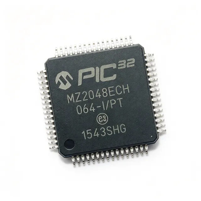
Quick Answers — What Is the PIC32MZ2048ECH064-I/PT?
The Microchip PIC32MZ2048ECH064-I/PT is a 32-bit PIC32MZ Embedded Connectivity microcontroller with a 200 MHz MIPS32 M-Class core, 2 MB of program Flash, and 512 KB of SRAM. It integrates a 10/100 Ethernet MAC, HS USB 2.0 host/device/OTG, two CAN 2.0B controllers, a 12-bit ADC rated at up to 18 MSPS, a hardware crypto engine, and 32 DMA channels. The device operates from 2.3 V to 3.6 V and is available in a 64-pin TQFP measuring 10 x 10 mm with a 0.5 mm pitch. XAIPART records 16,000 units in stock with an MOQ of 1. Its lifecycle status is NRND, with end-of-life scheduled for January 2027. The database lists a $7.15 base price as of 2026-11-01, while its quantity-1 pricing tier lists $12.18 as of 2026-11-01.
Review the PIC32MZ2048ECH064-I/PT product record before committing a new PCB because the component is no longer recommended for new designs. Existing connected products can use its Ethernet, USB, CAN, memory, and security resources, but buyers should qualify the PIC32MZ EF family for new programs.
Action: Use the EC variant for compatible legacy programs, confirm available inventory and lead time, and reserve a migration path for production after January 2027.
Technical Guide — How Do You Select and Design In the PIC32MZ2048ECH064-I/PT?
Begin with workload partitioning. The 200 MHz MIPS32 M-Class core provides up to 252 DMIPS and 3.28 CoreMark/MHz, while 32 DMA channels—8 dedicated and 24 shared—move data among peripherals, SRAM, and external memory without requiring every transfer to execute on the CPU. For network equipment or control systems, this combination determines whether protocol processing, control loops, and display or storage operations can coexist without exhausting memory or processor time.
| Resource | Verified capability | Design relevance |
|---|---|---|
| Processor | MIPS32 M-Class, up to 200 MHz, up to 252 DMIPS | Handles protocol stacks, application logic, and real-time control |
| Program memory | 2 MB, or 2048 KB, dual-panel Flash | Stores boot code, application code, drivers, and update images |
| Data memory | 512 KB SRAM | Buffers network packets, samples, frames, and protocol state |
| Ethernet | 10/100 MAC with MII/RMII | Requires an external Ethernet PHY for the physical layer |
| USB | HS USB 2.0 host, device, and OTG | Supports host, device, and OTG product architectures |
| CAN | Two CAN 2.0B controllers | Requires external CAN transceivers for bus connections |
| Analog conversion | 12-bit ADC, up to 48 channels, 18 MSPS | Acquires control and monitoring signals |
| Security | AES, 3DES, SHA, MD5, and RNG hardware engine | Offloads supported cryptographic operations |
| Package and I/O | 64-pin TQFP, 10 x 10 mm, 0.5 mm pitch, 53 I/O pins | Supports compact, mixed-signal industrial boards |
Check pin availability before committing the layout. The 64-pin package exposes Ethernet, USB, CAN, UART, I2C, parallel-interface, analog, clock, programming, and power functions, but it does not expose every function associated with larger variants in the family. Review the XAIPART component catalog and the device pin map during schematic capture. Ethernet PHY, USB connector, and CAN transceiver assignments can change board partitioning, so verify each signal against the exact 64-pin pinout rather than assuming that the full family pinout fits.
Plan the power tree around the verified 2.3 V to 3.6 V operating range. Place a 0.1 uF ceramic capacitor as close as possible to each VDD pin and add a 4.7 uF bulk capacitor on each main rail. The analog supply requires an additional 0.1 uF and 10 uF pair, with a ferrite bead separating it from digital noise. Keep the PLL filter capacitor network within 5 mm of the VDDPLL pin. These placement requirements reduce assembly-dependent supply problems that software changes cannot correct.
Use the dual-panel Flash and DMA resources as part of the product architecture, not merely as capacity figures. The dual-panel Flash supports live firmware updates without halting the application. For USB update or logging products, that arrangement can separate a bootloader and USB driver from the active application. The DMA controller can move USB endpoint data, ADC samples, and display data while the core handles application logic. Keep firmware, drivers, and update partitions aligned with the 2 MB Flash budget.
For an Ethernet gateway, the 512 KB SRAM provides 262,144 16-bit words when represented as two bytes per word. That capacity supports packet buffers and application state, although the final allocation must also reserve space for the protocol stack, DMA descriptors, and application variables. The 200 MHz core supplies 10,000 clock cycles in each 20 kHz control-loop period, a useful sizing baseline for the motor-control use case identified in the verified application data. Use actual interrupt latency, stack depth, and DMA contention to determine whether the selected loop rate leaves sufficient margin.
Analog designs should use the 12-bit, 18 MSPS ADC capability deliberately. The verified application data identifies simultaneous three-phase current and voltage sampling for motor control, with DMA streaming samples into SRAM. Preserve analog signal conditioning, grounding, and supply separation around the AVDD and AVSS pins. The MCU can expose up to 48 ADC channels, but the 64-pin package also has to accommodate Ethernet, USB, CAN, clocks, programming, and power pins, so verify the actual channel allocation before fixing the footprint.
Use the documented development path during firmware bring-up. The verified data lists MPLAB X, MPLAB Harmony v3, the XC32 compiler, the PIC32MZ Embedded Connectivity Starter Kit, MPLAB ICD 4, MPLAB Snap, and PICkit 4. Harmony provides TCP/IP, USB, and graphics stacks with middleware for the EC peripherals. The PIC32MZ EC Family Data Sheet, document 60001191G, remains the primary electrical, package, and pin-reference document.
Action: Freeze the pin allocation, power-decoupling layout, external PHY and transceiver selections, and memory budget before PCB release; then validate firmware with the supported MPLAB toolchain and the manufacturer data sheet.
Alternatives & Comparison — Which Drop-In Alternatives Are Available?
The verified migration path points to the PIC32MZ2048EFH064-I/PT for legacy EC-family programs. It retains the 64-pin TQFP footprint, 2 MB Flash, and 512 KB SRAM, but increases the maximum clock to 252 MHz and adds a single-precision IEEE-754 FPU. The verified guidance states that no PCB changes are required, although firmware must be recompiled for the successor's core features. Use this option when firmware compatibility and board continuity matter more than maintaining the exact EC processor implementation.
The PIC32MZ1024ECG064-I/PT offers a different engineering tradeoff. It uses the same 64-pin TQFP footprint and is pin-to-pin compatible, but provides 1,024 KB of Flash instead of 2,048 KB, 256 KB of SRAM instead of 512 KB, and no Ethernet. It is a footprint-compatible option, not a functional substitute for an Ethernet-connected design. The reduced memory also prevents a direct assumption that existing bootloaders, graphics assets, or network stacks will fit without modification.
| Parameter | PIC32MZ2048ECH064-I/PT | PIC32MZ2048EFH064-I/PT | PIC32MZ1024ECG064-I/PT |
|---|---|---|---|
| Maximum CPU clock | 200 MHz | 252 MHz | Not stated in provided comparison data |
| Performance | Up to 252 DMIPS; 3.28 CoreMark/MHz | Not stated in provided comparison data | Not stated in provided comparison data |
| Program Flash | 2 MB, or 2048 KB | 2 MB | 1,024 KB |
| SRAM | 512 KB | 512 KB | 256 KB |
| Floating-point unit | No FPU | Single-precision IEEE-754 FPU | Not stated in provided comparison data |
| Package | 64-pin TQFP, 10 x 10 mm, 0.5 mm pitch | 64-pin TQFP | 64-pin TQFP |
| Ethernet | 10/100 MAC with MII/RMII | Not stated in provided comparison data | No Ethernet |
| PCB transition | Existing EC-family design | No PCB changes; recompile firmware | Pin-to-pin compatible, but function and memory are reduced |
Do not classify the G variant as a drop-in replacement simply because the package matches. Its Flash and SRAM are each 50% lower than the ECH064, and the absence of Ethernet removes a defining feature of the connected EC device. The verified ECH064-to-EFH064 relationship is the closer migration choice when the board must remain unchanged.
Action: Select the EFH064 for an unchanged-board performance and FPU migration, and treat the G variant as a reduced-resource alternative only when Ethernet and the larger memory requirements are removed.
Industry Insight — What Does the Lifecycle and Supply Data Mean?
The component's lifecycle position is the central sourcing fact. XAIPART records the PIC32MZ2048ECH064-I/PT as NRND, meaning it is not recommended for new designs. The verified lifecycle information also identifies January 2027 as the scheduled end-of-life point. This status does not mean that every shipment is immediately unavailable, but it changes how buyers should allocate inventory and engineering effort. A product that is still building today needs a controlled migration plan rather than an assumption of indefinite supply.
The current database snapshot records 16,000 units in stock and an MOQ of 1. The verified sourcing information also states that distributor lead times may be 8-12 weeks as of 2026-10-04, while some distributors show in-stock inventory. These statements are not necessarily contradictory: one describes the XAIPART stock snapshot, and the other describes distributor conditions that can vary. Buyers should request a confirmed allocation and delivery schedule for their required quantity rather than extrapolating from the aggregate stock figure.
Pricing requires similar care. The verified database lists a $7.15 base price as of 2026-11-01, while the pricing table lists $12.18 at quantities of one or more as of 2026-11-01. Additional verified tiers are $10.95 at 10 units, $9.62 at 100 units, $8.42 at 500 units, and $7.15 at 1,000 units, all as of 2026-11-01. Because the base-price field and the one-unit tier differ, procurement documents should identify both the tier and the as-of date. Do not compare the $7.15 base field with a one-unit distributor quote without labeling the data source.
Manufactured demand should be treated as finite. The combination of an industrial -40 C to +85 C temperature range, RoHS-compliant status, MSL Level 3 handling, Ethernet, HS USB, CAN, and a hardware crypto engine supports connected industrial and commercial equipment. Nevertheless, the verified lifecycle recommendation directs new designs toward the PIC32MZ EF family. The EC part's value is strongest in installed programs and controlled continuation projects where firmware, certification, or PCB continuity carries more weight than access to the newest core.
For supply planning, separate three needs: immediate prototype availability, scheduled production quantities, and post-January 2027 continuity. The current 16,000-unit stock figure may address some near-term demand, but the verified data does not provide a complete date-by-date allocation schedule. Confirm quantity, packaging, price, and lead time for each production build. Do not let prototype stock obscure the lifecycle deadline.
Action: Place a time-bound migration plan ahead of January 2027, lock sufficient inventory for committed production, and require distributors to confirm allocations against each scheduled build rather than relying on the aggregate 16,000-unit stock snapshot.
Trends & Outlook — What Should Buyers Monitor?
Watch the shift from the EC family toward the EF family because the verified replacement path combines a higher 252 MHz clock, a single-precision FPU, the same 64-pin TQFP package, and unchanged 2 MB Flash and 512 KB SRAM capacity. This migration improves processing headroom and adds floating-point hardware without requiring a PCB change. It is especially relevant to control, networking, and signal-processing programs where the additional computation can replace software floating-point work or reduce application overhead. Review the new core features during recompilation and regression-test all peripheral behavior before production release.
Memory configuration remains a decisive product constraint. The ECH064 provides 2 MB of dual-panel Flash and 512 KB of SRAM, while the G alternative provides 1,024 KB and 256 KB. New firmware should include a memory budget for its bootloader, drivers, network stack, graphics assets, update image, and runtime buffers. Connected designs should also account for DMA descriptors and protocol buffers rather than treating all 512 KB as freely available application memory. The larger EC memory footprint remains one reason to preserve the ECH064 for established code or migrate to the equally sized EFH064 rather than the reduced G part.
Connectivity integration remains central to device selection. The MCU combines a 10/100 Ethernet MAC, HS USB 2.0 host/device/OTG, two CAN 2.0B controllers, multiple UART, SPI, and I2C channels, a parallel memory interface, and 53 I/O pins. This allows designers to consolidate gateways, USB peripherals, CAN nodes, and HMIs, but Ethernet and CAN still require external physical-layer devices. Select the PHY and transceiver early because their clock, data, control, and power requirements affect the 64-pin signal budget and board partitioning.
Security-aware connected products should account for the dedicated AES, 3DES, SHA, MD5, and RNG engine. The 2 MB Flash can hold security-aware boot code and application firmware, while dual-panel Flash supports live updates. Verify the exact firmware architecture, update process, and use of the hardware engine in the target stack; the presence of a crypto engine alone does not define a complete product security architecture.
Watch power and thermal requirements as designs increase peripheral activity. The verified application data identifies approximately 240 mW with Ethernet and other peripherals active, approximately 280 mW with the crypto engine active at full load, and approximately 310 mW with graphics, USB, and CAN active. These are application-table estimates, not guaranteed worst-case limits, so use them for early architecture planning and verify the final operating envelope against the device data sheet and actual board behavior.
Finally, monitor lifecycle notices and distributor inventory as leading indicators, not just price changes. A falling unit price can reflect excess inventory rather than a healthy long-term supply position. The relevant questions are whether the quantity can be allocated, whether production lead time remains acceptable, and whether the order can be delivered before the January 2027 end-of-life point. For additional engineering context, the XAIPART article on AI-assisted microcontroller prototyping is useful background, but device selection should remain anchored to the verified PIC32MZ data.
Action: Prioritize a same-footprint EFH064 migration for new programs, preserve the ECH064 only where firmware or board continuity justifies it, and track delivery allocation, lifecycle notices, memory demand, and peripheral power together.
Bình luận
Trở thành người đầu tiên bình luận.
🔐 Vui lòng đăng nhập để đăng một bình luận.
Bạn không có tài khoản? Đăng ký