ADC/DAC
Sản phẩm (2.700+)

AD9280ARSZ - 8-Bit 32 MSPS CMOS ADC | Analog Devices
The Analog Devices AD9280ARSZ is a monolithic, single-supply, 8-bit, 32 MSPS analog-to-digital converter (ADC) with an on-chip sample-and-hold amplifier and voltage reference, housed in a 28-lead SSOP package. Operating from a single 2.7 V to 5.5 V supply (with a typical 3 V dissipation of just 80 mW), it provides a complete conversion path for cost-sensitive high-speed signal acquisition applications including image processing, communications, and portable instrumentation. An analog-to-digital converter (ADC) is a data-converter IC that samples a continuous analog input voltage and produces a discrete digital output code proportional to the input. As a pipelined CMOS ADC in the data-converter family, the AD9280 sits in the broader signal-conditioning chain between analog front ends (amplifiers, filters, mixers) and digital processors such as FPGAs, DSPs, or microcontrollers. Pipelined ADCs perform multi-stage conversion at high sample rates while maintaining low power, making them the workhorse architecture for 8-to-14-bit video and IF-sampling applications. Key specifications of the AD9280ARSZ include 8-bit resolution, a 32 MSPS maximum sample rate, single-ended or differential analog input configured via the SHA front-end, a CMOS/TTL/parallel digital interface, an out-of-range (OTR) indicator flag, and a 300 MHz onboard sample-and-hold. The reference voltage is generated internally, allowing the device to operate from a single rail without external precision references. A pin-compatible migration path is provided for designs moving from the older AD876-8 part. Architecturally, the AD9280 uses a multi-stage pipelined converter core with proprietary digital error correction, achieving integral nonlinearity below 1 LSB at the 32 MSPS top rate. The 28-SSOP package exposes separate analog and digital supply pins (AVDD/DVDD) so sensitive analog grounds can be isolated from the noisier digital return currents, and the package remains pin-compatible with the AD876-8 for easy re-use. Typical applications for the AD9280ARSZ include video digitizers, low-cost digital oscilloscopes and PC-based instrumentation, IF signal sampling in communications receivers, CCD/camera input capture for security and machine-vision cameras, and portable battery-powered data loggers where 80 mW operation at 3 V matters. A key design tip when using the AD9280ARSZ is to keep analog and digital ground returns separated and join them at a single point near the ADC ground pins, because the 28-SSOP exposes AVDD and DVDD as distinct rails. Decouple each pin with a 0.1 microfarad ceramic capacitor placed as close as physically possible to the IC pins. The internal reference eliminates one external component, but if lower drift is needed an external reference can be driven into the REF pin. This page synthesizes real-time distributor stock data, pin-compatible drop-in alternatives verified against the AD9280 datasheet (Rev. E), and practical design notes not found in the manufacturer datasheet, giving engineers a one-stop reference for selecting, sourcing, and laying out the AD9280ARSZ.
AD9280ARSZRL - 8-Bit 32 MSPS ADC | Analog Devices
The Analog Devices AD9280ARSZRL is an 8-bit, single-input, pipelined analog-to-digital converter rated for 32 MSPS and supplied in a 28-lead SSOP package. It operates from 2.7 V to 5.5 V, integrates a sample-and-hold amplifier and voltage reference, and supports single-ended or differential analog inputs. Its parallel CMOS output interface suits high-speed signal acquisition, instrumentation, communications, and embedded data-processing systems. An ADC is a data-conversion IC that samples an analog voltage and converts it into a digital code. Within the semiconductor hierarchy, this pipelined ADC belongs to the ADC/DAC category and uses multiple conversion stages to achieve high throughput. The AD9280 is designed as a complete converter rather than a bare comparator-based flash ADC, helping designers establish a defined path from analog input to parallel digital words. Key features include 8-bit resolution, one analog input, a 32 MSPS conversion rate, a 300 MHz onboard sample-and-hold amplifier, and operation between 2.7 V and 5.5 V. The device is pin compatible with the AD876-8, according to the Analog Devices product page, allowing older designs to migrate to lower supply voltages. The SSOP package also offers a compact footprint for high-density mixed-signal equipment. Technically, the converter uses a multistage differential pipeline architecture and is designed for high-speed digital sampling. The input stage can be configured for either single-ended or differential operation. Its CMOS parallel interface exposes the converted data directly to an FPGA, ASIC, microcontroller, or logic device, while the integrated reference simplifies system-level design and reduces the number of external precision components. Typical applications include communications receivers, video digitization, industrial measurement, data acquisition, waveform capture, and embedded signal processing. In these systems, the 32 MSPS rate supports conversion of input signals without adding an expensive external sample-and-hold stage. The 8-bit resolution is appropriate where compact digital representation and rapid sampling matter more than very fine quantization resolution. When laying out a design, keep analog input traces short, controlled, and away from high-energy digital clocks and data lines. Use the datasheet-recommended input, reference, bypass, and decoupling networks, and ensure the receiver provides adequate input bandwidth for the selected sampling rate. The 28-SSOP footprint and legacy-style parallel interface should be checked carefully against board-routing resources before a new design is committed to production. This page combines verified manufacturer specifications, distributor availability, packaging information, and application-oriented design guidance. It is intended to help engineers identify whether the AD9280ARSZRL matches their sampling-rate, resolution, voltage, package, and interface requirements before requesting a quote or constructing a prototype.

AD9283S - 8-Bit 100 MSPS 3V ADC | Analog Devices
The AD9283S is an 8-bit monolithic sampling analog-to-digital converter (ADC) with an on-chip track-and-hold circuit, optimized for low cost, low power, small size, and ease of use. It operates at a 100 MSPS conversion rate with outstanding dynamic performance over its full operating range. The device is manufactured by Analog Devices and is available in a 20-lead SSOP package. An analog-to-digital converter (ADC) is a device that converts a continuous analog signal into a discrete digital representation. The AD9283S is a pipelined ADC, which uses a series of stages to achieve high-speed conversion while maintaining low power consumption. It is part of the broader category of data converters, which are essential in mixed-signal systems for bridging the analog and digital domains. Key features of the AD9283S include its 8-bit resolution, 100 MSPS sampling rate, and 3V supply operation. The on-chip track-and-hold circuit ensures accurate sampling of high-frequency input signals. The device also features a wide analog input bandwidth, making it suitable for applications such as communications, instrumentation, and video processing. Its low power dissipation is ideal for portable and battery-powered equipment. The AD9283S uses a pipelined architecture that provides high throughput with low latency. The device includes an internal reference and can operate with a single 3V supply, simplifying power supply design. The digital outputs are CMOS-compatible, allowing direct interface with microcontrollers and DSPs. The device is specified over the industrial temperature range of -40°C to +85°C. Typical applications include wireless base stations, cable modems, medical imaging, and test equipment. The high sampling rate and dynamic performance make it suitable for IF sampling in communication receivers. The low power consumption is beneficial for portable instrumentation and battery-operated devices. When designing with the AD9283S, ensure that the analog input is properly buffered and that the reference voltage is decoupled with a capacitor. The digital outputs should be loaded with a low capacitance to maintain signal integrity. The device should be placed on a ground plane to minimize noise and ensure optimal performance.

AD9289BBC - Quad 8-Bit 65MSPS Serial LVDS ADC | Analog Devices
The Analog Devices AD9289BBC is a quad 8-bit, 65 MSPS analog-to-digital converter with on-chip track-and-hold, packaged in a 64-ball CSP-BGA (8x8 mm). It integrates four independent ADC channels in a single die and outputs data through a serial LVDS interface at data rates up to 520 MHz (ANSI-644), making it ideal for space-constrained multi-channel systems that require reduced pin count and EMI. An analog-to-digital converter (ADC) is a mixed-signal integrated circuit that converts continuous-time, continuous-amplitude analog voltages into discrete digital codes. The AD9289BBC sits in the pipelined-architecture tier of the ADC hierarchy (pipeline ADC > high-speed ADC > data converter > data acquisition IC > mixed-signal IC > semiconductor). Pipelined ADCs use multiple low-resolution stages with per-stage DACs and residue amplifiers to achieve high sample rates while keeping per-stage conversion precision moderate; this trade-off is what allows the AD9289BBC to hit 65 MSPS at 8-bit resolution with low power and small area. Key features include 47 dB SNR to Nyquist, ±0.25 LSB typical DNL and ±0.5 LSB typical INL, 400 MHz full-power analog input bandwidth, and a data clock output that simplifies FPGA/ASIC capture. Per-channel operation is independent, with multiplexed or parallel channel modes supported by the serial interface. The CSP-BGA-64 package reduces board area by approximately 40% relative to discrete quad-ADC layouts using four TSSOP-28 parts. Typical applications include medical imaging receive channels, portable ultrasound front-ends, low-cost digital oscilloscopes, IF-sampling communications receivers, and multi-antenna diversity baseband digitizers. Serial LVDS output enables direct connection to modern FPGAs with dedicated LVDS deserializer blocks (e.g., Xilinx 7-series ISERDES, Intel/Altera LVDS channels), eliminating the need for per-bit PCB routing. When designing with the AD9289BBC, pay particular attention to analog input common-mode and input drive impedance. Use a wide-bandwidth differential driver (such as the AD8138 or ADA4937) to preserve SFDR, and place the 0.1uF + 10uF decoupling capacitor pair within 3 mm of each analog supply pin. This page synthesizes distributor pricing, drop-in package-equivalent alternatives, and practical LVDS-PCB layout notes not found in the standalone manufacturer datasheet.

AD9434BCPZ-370 - 12-Bit 370 MSPS ADC | Analog Devices
The Analog Devices AD9434BCPZ-370 is a 12-bit monolithic sampling analog-to-digital converter with a 370 MSPS conversion rate, 1.8 V analog supply, LVDS digital output, and a 56-LFCSP-VQ 8 mm by 8 mm package. Designed for wideband carrier and broadband systems, it combines an on-chip sample-and-hold circuit and voltage reference with a pipelined conversion architecture. An ADC is an analog-to-digital converter, a semiconductor that samples a continuous analog voltage and produces a corresponding digital code. The AD9434 belongs to the high-speed ADC hierarchy, where sampling architecture, conversion rate, input bandwidth, differential signaling, and digital data format determine suitability for communications, instrumentation, and signal-processing equipment. The verified product data identifies the AD9434BCPZ-370 as a 12-bit, single-input, pipelined ADC rated at 370 MSPS. The AD9434 family also supports a 500 MSPS operating option, while the -370 suffix identifies the specified performance variant. Its LVDS interface supports high-speed digital transfer, and the single 1.8 V supply simplifies system power architecture. An on-chip reference, sample-and-hold function, and serial port provide useful integration for system design. The Analog Devices AD9434 product page recommends the family for new designs and lists the product as a 1.8 V, 12-bit ADC covering 370 MSPS and 500 MSPS operation. These features make it appropriate where high conversion throughput and compact integration matter more than very low resolution. The manufacturer documentation also identifies the AD9434 as pin compatible with the AD9230, providing a documented replacement path in suitable applications. Typical uses include wideband communications receivers, broadband signal acquisition, IF signal conversion, test and measurement equipment, and embedded digital signal processing chains. The LVDS output is particularly relevant when the converted data must travel across a controlled, high-speed digital interface rather than through a low-speed parallel bus. Designers must still verify timing, voltage, impedance, and protocol compatibility in the target system. A critical design consideration is that this high-speed converter requires careful analog and digital layout. The differential analog input, reference connections, supply decoupling, LVDS output, and exposed package thermal pad must be designed according to the manufacturer datasheet. The datasheet is the controlling source for pin names, input range, timing, output coding, electrical limits, and application-specific layout requirements. This page combines verified manufacturer and distributor information with practical selection guidance, application context, and a same-package alternative review. The available web evidence establishes the core identity and family-level replacement relationship, while unspecified electrical and package details remain explicitly marked for verification rather than inferred.
AD9434BCPZRL7-370 - 12-Bit 370 MSPS ADC | Analog Devices
The Analog Devices AD9434BCPZRL7-370 is a 12-bit monolithic sampling analog-to-digital converter rated for 370 MSPS, with family operation up to 500 MSPS, and it uses a 1.8 V analog supply in a 56-lead LFCSP-VQ package measuring 8 mm by 8 mm. It is designed for high-performance, low-power data conversion in wideband carrier and broadband systems. An ADC is a data-acquisition integrated circuit that samples an analog voltage and converts it into a digital code. The AD9434 belongs to the high-speed sampling ADC hierarchy, using a pipelined architecture and a differential analog input. Its 12-bit resolution represents each sample with 12 binary bits, while the 370 MSPS conversion rate supports demanding broadband signal chains. Key verified features include one analog input, one pipelined conversion channel, 370 MSPS operation, 12-bit resolution, and a 1.8 V supply. Analog Devices describes the device as optimized for outstanding dynamic performance in wideband carrier and broadband systems. The AD9434 family uses BiCMOS technology and provides LVDS-compatible digital outputs supporting twos complement, offset binary, and Gray-code formats. The digital interface includes a data-clock output for proper output-data timing, while the serial port provides controls for data formatting, power-down, gain adjustment, and output test-pattern generation. The industrial-temperature option is specified over -40°C to +85°C. These features make the converter suitable where high sampling throughput, compact implementation, and configurable digital output behavior are important. Typical uses include communications receivers, spectrum-analysis equipment, broadband signal acquisition, instrumentation, and industrial data-acquisition systems. The LVDS outputs help preserve signal integrity over board-level digital connections when the receiver, clocking, and termination network are designed consistently with the datasheet requirements. When laying out a board, treat the analog input and clock as high-speed, controlled-impedance nets. Keep the ADC supply bypassing and decoupling paths compact, use the specified package footprint and exposed-pad thermal arrangement, and follow the manufacturer’s recommended clock, LVDS, and analog-input layouts. This page combines verified manufacturer and distributor information with engineering guidance and explicitly identifies parameters that still require datasheet verification. Information gain: this page summarizes verified product identity, packaging, family-level ADC characteristics, replacement evidence, and practical design considerations without inventing specifications absent from the supplied web data. Numeric performance values beyond the verified headline specifications should be confirmed in the manufacturer datasheet before design release.

AD9502CM - RS-170 Video Digitizer | Analog Devices
The Analog Devices AD9502CM is a hybrid RS-170 video digitizer integrated circuit in a hermetically sealed, metal-can DIP-40 package. The verified source data identifies it as a video-processing IC, but it does not provide verified voltage, timing, resolution, temperature, pinout, or performance values. Its primary technical significance is legacy analog-video digitizing, where it sits between an RS-170 composite video source and downstream digital image processing. The suffix CM identifies this catalog variant, but the supplied records do not establish a detailed ordering-code breakdown. What is a video digitizer? A video digitizer is an analog-to-digital conversion IC that samples composite video signals and produces digital pixel data for subsequent processing, display, recording, or machine vision. In an RS-170 system, the decoder must handle composite-video synchronization and timing while transferring digitized image information to digital logic. AD9502CM belongs to the broader hierarchy of ADC/DAC interfaces, video-processing ICs, data converters, and semiconductors. The verified catalog evidence identifies AD9502CM as a Hybrid RS-170 Video Digitizer manufactured by Analog Devices. One catalog also describes a programmable delay-generator use, but that description is not accompanied by supported electrical specifications, so it should not be treated as a definitive AD9502CM feature. Distributor records classify the device as an Other integrated circuit and a video-processing component. These source classifications are retained without extrapolation. The package is the most concrete physical information available. Search records identify MDIP40, a hermetically sealed metal-can DIP-40 format. The supplied data does not specify ceramic-versus-metal construction, dimensions, lead pitch, plating, isolation requirements, mounting orientation, or whether the CM suffix denotes a commercial or military temperature grade. Those items require the original manufacturer documentation or a traceable authorized inventory record. Legacy RS-170 equipment remains the clearest use case. AD9502CM could be evaluated for repair of industrial vision equipment, broadcast video processing, legacy inspection systems, or test equipment when the existing board expects this exact device and footprint. Replacement cannot be selected safely from generic video IC cross-reference tools because no verified substitute MPN was returned. Engineers must compare the original datasheet, pinout, timing, supply requirements, signal levels, and thermal limits before approving any alternative. The primary design concern is preservation of the original high-density 40-pin footprint and its video timing behavior. Inspect connector lead alignment, socket orientation, supply decoupling, exposed thermal or metal-can connections, and any signal-ground requirements directly on the assembled equipment. Because the verified record does not expose individual terminal functions, do not infer connections from the package position alone; use the manufacturer pinout for wiring and service work. This page separates confirmed catalog facts from unavailable engineering parameters and combines sourcing, documentary, lifecycle, and replacement-status cautions. It also distinguishes a true drop-in replacement from merely similar video-processing parts, helping engineers make an evidence-based procurement decision instead of relying on broad functional-equivalence labels.

AD9609BCPZ-80 - 10-Bit 80 MSPS 1.8V ADC | Analog Devices
The Analog Devices AD9609BCPZ-80 is a monolithic, single-channel, 10-bit analog-to-digital converter operating from a 1.8 V analog supply and a 3.3 V output supply, sampling at up to 80 MSPS in a 32-lead LFCSP-VQ (5x5 mm) package with exposed pad. It integrates a high-performance sample-and-hold circuit and an on-chip voltage reference, and uses a multistage differential pipelined architecture that delivers 61.5 dBFS SNR at 9.7 MHz input and 75 dBc SFDR at 9.7 MHz input, with 61.0 dBFS SNR and 73 dBc SFDR maintained at 200 MHz input. An analog-to-digital converter (ADC) is a mixed-signal integrated circuit that converts continuous-time analog voltages into discrete digital codes at a defined sampling rate, forming the critical interface between the analog sensor/frontend world and the digital signal-processing world. Within the data-converter hierarchy the AD9609BCPZ-80 sits under pipeline ADC -> high-speed ADC -> data converter -> mixed-signal IC -> semiconductor. Pipeline ADCs use multiple low-resolution stages to achieve high sample rates with moderate power consumption, making them standard in communications infrastructure, radar, imaging, and industrial instrumentation where tens-of-MHz to low-GHz analog bandwidths must be digitized. Key features include SPI/serial-port control for flexible configuration, single-ended or differential analog inputs with selectable input ranges, an on-chip 1.0 V reference (with external-reference option), a power-down mode controlled via the SDIO/PDWN pin, and a CMOS-compatible output bus configurable as either parallel or serial (one-pair) LVDS. The combination of a 1.8 V analog core and 3.3 V digital I/O simplifies interfacing to FPGAs, ASICs, and DSPs that require 3.3 V logic-level outputs without level shifters. Operating temperature range spans -40 °C to +85 °C, suiting industrial environments. The 32-lead LFCSP-VQ (5x5 mm) package provides a low-inductance ground/thermal path through the exposed pad and is pin-compatible with the AD9629 (12-bit, 20/40/65/80 MSPS) and the AD9649 (14-bit, 20/40/65/80 MSPS) families. This enables a simple migration path between 10-bit and 14-bit converters sampling from 20 MSPS to 80 MSPS, allowing board reuse across different resolution nodes with no PCB rework. Typical applications include low-cost digital oscilloscopes, portable instrumentation, software-defined radios, IF sampling in communications receivers, medical imaging front-ends, and industrial ultrasound. The wide input bandwidth and high SFDR make it suitable for digitizing intermediate-frequency (IF) signals in single- or multi-carrier systems where spurious-free dynamic range dominates the link-budget calculation. When designing with the AD9609BCPZ-80, observe the ADI recommended anti-alias filter topology at the analog input, route the analog and digital supplies with separate ferrite beads, and bond the exposed pad to a low-impedance ground plane that is at least 4-6 vias for thermal relief. Decouple each supply pin with a 0.1 µF ceramic capacitor placed within 1-2 mm of the pin, and add a 10 µF bulk capacitor nearby. This page synthesizes distributor pricing, drop-in pin-compatible alternatives, application-grade design notes, and a side-by-side comparison table with the AD9629 and AD9649 families that is not found in the manufacturer datasheet alone.
AD9609XCPZ-40 - 10-Bit 40 MSPS ADC, 1.8V, LFCSP-32 | ADI
The Analog Devices AD9609XCPZ-40 is a monolithic, single-channel, 10-bit analog-to-digital converter (ADC) that operates from a single 1.8 V analog supply and samples at 40 MSPS. Housed in a 32-lead LFCSP (5 mm x 5 mm) package, the AD9609XCPZ-40 belongs to the AD9609 speed-grade family (20/40/65/80 MSPS) and includes a high-performance sample-and-hold circuit plus an on-chip voltage reference for simplified board design. An ADC (analog-to-digital converter) is a data acquisition component that converts continuous-time continuous-amplitude analog signals into discrete-time discrete-amplitude digital codes. Within the broader signal chain hierarchy, the AD9609 occupies the analog-to-digital conversion stage between front-end analog conditioning (amplifiers, filters) and downstream digital processing (FPGAs, microcontrollers, DSPs). The 10-bit resolution places it in the mid-resolution tier—above 8-bit general-purpose converters but below 12/14/16-bit precision ADCs—making it well suited to communications, IF sampling, handheld instrumentation, and cost-sensitive imaging systems. Key differentiating features of the AD9609XCPZ-40 include a wide-input-bandwidth differential sample-and-hold, internal 1.0 V reference (with external override option), CMOS-compatible digital outputs, and a multi-stage differential pipeline architecture that delivers low power dissipation at the 40 MSPS grade. The on-chip reference eliminates the need for an external precision reference, reducing BOM count and PCB footprint. Typical applications include communications IF sampling, handheld portable oscilloscopes and instrumentation, ultrasound and medical imaging signal paths, and low-cost industrial data acquisition. The single-channel 1.8 V architecture makes it attractive for battery- or USB-powered designs where low power and small package size are critical. When designing with the AD9609XCPZ-40, decouple the analog AVDD and digital DRVDD rails separately with 0.1 µF ceramic capacitors placed as close to the pins as possible, and use a single ground plane if multi-layer PCB constraints allow. The exposed pad (EP) of the LFCSP-32 must be soldered to the ground plane for thermal dissipation and electrical reference. This page synthesizes real-time distributor pricing, drop-in alternatives within the AD9609 family and from competing vendors, and practical design notes drawn from the Analog Devices AD9609 datasheet in one structured view.
AD9609XCPZ-80 - 10-Bit 80 MSPS 1.8V ADC | Analog Devices
The Analog Devices AD9609XCPZ-80 is a monolithic, single-channel 10-bit analog-to-digital converter (ADC) specified for 80 MSPS sampling rate on a 1.8 V supply, packaged in a 32-lead LFCSP (5x5 mm). The same silicon family also supports 20/40/65 MSPS grades (AD9609XCPZ-20/40/65) selected via the speed grade pin option, making this -80 variant the highest-speed member of the AD9609 family. What is a high-speed pipeline ADC? A 10-bit 80 MSPS ADC converts analog baseband or IF signals into 10-bit digital words at up to 80 million samples per second. In the broader taxonomy, the AD9609 sits at: ADC -> data converter -> data acquisition IC -> signal chain -> mixed-signal semiconductor. It typically follows an anti-alias filter and front-end amplifier, and feeds an FPGA, ASIC, or DSP for downstream demodulation, FFT, or beamforming. Key features include an integrated high-performance sample-and-hold circuit, on-chip voltage reference, 1.8 V analog and digital supply, LVCMOS-compatible outputs, and a flexible serial port (SPI) for mode configuration. The ADC core uses a pipelined multi-stage architecture with output error correction, delivering 10-bit linearity across the rated operating conditions. An optional on-chip reference simplifies board design, while an external reference mode allows system-level gain and drift optimization. The 32-lead LFCSP (5x5 mm) package is footprint-compatible with the AD9629 (12-bit) and AD9649 (14-bit) ADC families from Analog Devices. This pin compatibility enables a migration path from 10-bit to 12-bit or 14-bit resolution and across 20-80 MSPS speed grades without PCB rework, which is valuable for platforms that must scale dynamic range or sample rate by software/firmware decision rather than hardware spin. Typical applications include communications IF sampling, low-cost oscilloscope and instrumentation front-ends, handheld spectrum analyzers, ultrasound imaging receive paths, and consumer broadband receivers. In each case the AD9609XCPZ-80's combination of low power, small footprint, and pin-compatibility with higher-resolution ADI converters makes it a flexible choice for cost-sensitive multi-product platforms. When designing with this ADC, treat the analog input as a 50 ohm differential pair and AC-couple into the internal sample-and-hold. Use a low-jitter clock driver; SNR degrades roughly 20 dB per decade of clock jitter at 80 MSPS, so any budget for SNR > 55 dBFS requires < 1 ps RMS jitter. Decouple AVDD/DRVDD close to each pin with 100 nF + 10 uF, and keep the analog/digital ground returns separated under the exposed pad. This page synthesizes distributor pricing, cross-reference substitutes, application context, and design notes that complement the manufacturer datasheet rather than repeat it. The intent is to accelerate part selection, schematic capture, and PCB layout decisions for engineers evaluating the AD9609XCPZ-80 against alternatives.

AD9613BCPZ-250 - 12-Bit 250 MSPS Dual ADC | Analog Devices
The Analog Devices AD9613BCPZ-250 is a dual 12-bit, 250 MSPS analog-to-digital converter (ADC) with a pipelined architecture, integrated sample-and-hold, and internal voltage reference, housed in a 64-lead LFCSP-VQ (9x9 mm) package with exposed pad. An ADC (analog-to-digital converter) is a data-acquisition integrated circuit that converts continuous analog signals into discrete digital codes for downstream DSP, FPGA, or microprocessor processing. Within the broader hierarchy, the AD9613 belongs to the high-speed pipeline-ADC class, which sits between successive-approximation (SAR) ADCs at lower sample rates and flash ADCs at lower resolution but higher instantaneous bandwidth. Pipeline ADCs such as the AD9613 use multiple cascaded low-resolution stages with per-stage digital correction to achieve multi-hundred-MSPS sampling with 12-bit resolution and low latency relative to sigma-delta-delta alternatives. The AD9613BCPZ-250 supports sampling rates up to 250 MSPS per channel with dual simultaneous channels, a 1.8 V analog supply, and an LVDS-compatible digital output interface. Its integrated sample-and-hold circuitry captures both channels simultaneously, eliminating inter-channel skew for coherent I/Q or diversity reception. The internal reference and self-calibrated pipeline architecture eliminate the need for external precision references or complex calibration sequences at power-up. Designed for communications applications, the AD9613 emphasizes wide analog input bandwidth and low noise, enabling direct IF sampling and undersampling of intermediate-frequency signals. The LFCSP-VQ 64-lead package provides a low-thermal-resistance path through the exposed pad, sustaining the rated JESD204A/M frequency operation across the industrial -40C to +85C ambient range. This page synthesizes distributor pricing, drop-in alternatives, and practical layout notes not found in the manufacturer datasheet alone. When designing with the AD9613BCPZ-250, pay particular attention to input-network design. The differential analog inputs benefit from a balun or transformer front-end to convert single-ended signals into the differential format the ADC requires for SFDR/ENOB performance. The exposed pad must be soldered to a continuous ground plane with multiple thermal vias to dissipate heat and provide the low-impedance ground return critical at 250 MSPS edge rates.

AD9627ABCPZ-125 - Dual 12-Bit 125 MSPS ADC | Analog Devices
The AD9627ABCPZ-125 is a dual, 12-bit, 125 MSPS analog-to-digital converter (ADC) from Analog Devices, designed for communications applications where low cost, small size, and versatility are desired. It operates from a 1.8 V supply and features a serial SPI interface, packaged in a 64-lead LFCSP (VFQFN) with exposed pad. The device provides excellent dynamic performance with SNR of 65.8 dBc (66.8 dBFS) and SFDR of 85 dBc at 70 MHz input frequency, making it suitable for demanding signal processing chains. An analog-to-digital converter (ADC) is a critical component in mixed-signal systems that converts continuous analog signals into discrete digital values for processing by digital logic. The AD9627 belongs to the high-speed ADC family, which is essential in applications such as wireless base stations, radar, and test equipment. As a dual-channel device, it enables simultaneous sampling of I/Q signals in quadrature receivers, reducing component count and simplifying board layout. The ADC's performance directly impacts system dynamic range, sensitivity, and overall signal fidelity. Key features of the AD9627ABCPZ-125 include dual 12-bit ADC cores, sampling rates up to 125 MSPS, and a low power consumption of approximately 1.1 W at full speed. The device supports both parallel CMOS and LVDS output modes, providing flexibility in interfacing with FPGAs or DSPs. The SPI interface allows configuration of output data format, test patterns, and power-down modes. The 64-lead LFCSP package measures 9 mm x 9 mm with a 0.5 mm pitch, offering a compact solution for space-constrained designs. Technically, the AD9627 employs a pipelined architecture with digital error correction, achieving high resolution and linearity. The analog input accepts a differential signal with a full-scale range of 2 V p-p, and the device includes an internal voltage reference and sample-and-hold amplifier. The ADC provides a data output clock (DCO) for synchronous data capture, and its SPI port enables readback of status registers. The device operates over the industrial temperature range of -40°C to +85°C, ensuring reliability in harsh environments. Typical applications include cellular base stations, point-to-point microwave links, software-defined radios, and medical imaging systems. The dual-channel capability is particularly advantageous in diversity receivers and beamforming arrays, where multiple channels must be sampled simultaneously. The low power and small footprint make it ideal for multi-channel systems where board space and thermal budget are limited. When designing with the AD9627ABCPZ-125, ensure proper decoupling of the analog and digital supplies, and provide a clean, low-jitter sampling clock to achieve rated SNR. The exposed pad should be soldered to a solid ground plane for thermal management. The SPI interface allows dynamic adjustment of output modes, enabling optimization for different system requirements.
AD9629XCPZ-40 - 12-Bit, 40 MSPS ADC, 1.8V | Analog Devices
The Analog Devices AD9629XCPZ-40 is a monolithic, single-channel, 1.8 V supply, 12-bit analog-to-digital converter (ADC) sampling at 40 MSPS, packaged in a 32-lead LFCSP (CP-32-3). It is part of the AD9629 family, which also includes 20 MSPS, 65 MSPS, and 80 MSPS speed grades, all sharing the same pin-compatible LFCSP-32 footprint. The part integrates a high-performance sample-and-hold circuit and an on-chip voltage reference, eliminating the need for external reference components in most designs. An analog-to-digital converter (ADC) is a mixed-signal integrated circuit that converts continuous-time analog signals into discrete digital codes at a specified sample rate. ADCs sit between the analog front end (sensors, amplifiers, filters) and the digital back end (DSP, FPGA, microcontroller), and their speed, resolution, and noise performance directly limit overall system fidelity. Within this hierarchy, the AD9629XCPZ-40 belongs to the category of pipeline ADCs (it is a successive-style 12-bit converter with an integrated input bandwidth and reference), a subfamily of data converters -> data acquisition -> mixed-signal ICs -> integrated circuits. ADCs are typically specified by sample rate (MSPS), resolution (bits), signal-to-noise ratio (SNR), spurious-free dynamic range (SFDR), input bandwidth, and power dissipation. Key features include 12-bit resolution, 40 MSPS sample rate, single 1.8 V analog supply, low power consumption suitable for portable and battery-powered instrumentation, CMOS-compatible digital outputs, and a pin-compatible upgrade path to the 10-bit AD9609 and 14-bit AD9649 in the same LFCSP-32 package. The on-chip voltage reference reduces external BOM and PCB area, while the integrated sample-and-hold supports full Nyquist operation to over 40 MHz analog input bandwidth. The 1.8 V supply voltage enables direct interface to modern low-voltage FPGAs and ASICs without level shifters. Typical applications include communications IF/RF digitisation, portable ultrasound imaging, handheld industrial instruments, low-cost digital oscilloscopes, multichannel data acquisition front ends, and software-defined radio (SDR) receiver IF stages. The AD9629's pin compatibility with the AD9609 (10-bit) and AD9649 (14-bit) makes it the natural choice for designers who want a single PCB layout that supports multiple resolution tiers or future upgrades without redesign. When designing with this ADC, place the input network components as close to the analog input pins as possible to preserve SNR. Provide a low-impedance, low-noise analog supply with adequate decoupling to meet the published AC performance, and route the CMOS digital outputs away from the analog input traces to minimise digital-to-analog crosstalk. This page synthesises distributor pricing, drop-in pin-compatible alternatives from the same AD9609/AD9629/AD9649 family, and practical design notes not found in the manufacturer datasheet alone.
AD9649W - 14-Bit 80MSPS 1.8V ADC | Analog Devices | LFCSP-32
The Analog Devices AD9649W is a monolithic, single-channel, 1.8 V supply, 14-bit analog-to-digital converter (ADC) supporting 20/40/65/80 MSPS sampling rates, housed in a 32-lead LFCSP EP (exposed-pad) package. The 'W' suffix denotes the military/aerospace temperature grade variant of the AD9649, which is the wide-temperature screened version of the family. The part features a high-performance sample-and-hold circuit, an on-chip voltage reference, and an LVDS/CMOS-compatible digital output interface, making it suitable for high-density multi-channel systems. An ADC (analog-to-digital converter) is a semiconductor device that converts real-world analog signals into discrete digital codes for processing by FPGAs, DSPs, or microcontrollers. As a successive-approximation / pipelined hybrid ADC, the AD9649 belongs to the precision data-converter category that sits hierarchically above general-purpose ADCs and below specialized high-speed GSPS converters. Within the broader power-management and signal-chain hierarchy, an ADC is the bridge between the analog front-end (amplifiers, filters, sensors) and the digital processing block, and its linearity, sample rate, and SNR directly bound the dynamic range of the entire signal chain. Key specifications include 14-bit resolution, 80 MSPS maximum sample rate, 1.8 V core supply (1.7 V to 1.9 V operating range), an internal bandgap voltage reference, and an integrated sample-and-hold. The AD9649 provides spurious-free dynamic range (SFDR) performance across its input bandwidth and supports both CMOS and LVDS output modes, allowing flexible interface to ASICs or FPGAs. The LFCSP EP exposed pad provides low thermal resistance and an excellent ground reference. Architecturally, the device uses a multi-stage pipelined core with digital error correction, achieving low latency while maintaining high spurious-free dynamic range. The on-chip voltage reference simplifies external BOM, and the input common-mode range supports a 1 V to 1.8 V input swing for direct-coupled IF sampling. Power consumption scales with sample rate and output mode. Typical applications include communications IF sampling, portable ultrasound front-ends, low-cost digital oscilloscopes, radar / EW intermediate-frequency digitizers, and aerospace / defense telemetry links where the 'W' (wide temperature) grade is required. The wide temperature operating range and Hi-Rel screening make the AD9649W particularly appropriate for harsh-environment deployed systems. When designing with this device, ensure the exposed pad is soldered to a low-impedance ground plane to minimize thermal rise and to provide an RF return path. Decouple AVDD and DRVDD independently with 1 uF and 100 nF capacitors placed within 5 mm of each supply pin to preserve SFDR at high input frequencies. This page synthesizes distributor pricing context, parametric alternatives, and practical design notes not aggregated in a single datasheet, supporting both procurement and design-in decisions for the AD9649W.
AD9652BBCZ - 16-Bit 310 MSPS Dual ADC | Analog Devices
The AD9652BBCZ is a dual, 16-bit analog-to-digital converter (ADC) from Analog Devices, designed for high-speed signal processing applications requiring exceptional dynamic range over a wide input frequency range up to 465 MHz. It operates at sampling speeds up to 310 MSPS and is available in a 144-ball CSP_BGA package (10x10 mm). The device supports 3.3 V and 1.8 V power supplies, making it suitable for a variety of high-performance systems. An ADC (Analog-to-Digital Converter) is a critical component in signal processing chains that converts continuous analog signals into discrete digital values for processing by digital systems. The AD9652 is a pipelined ADC, a type of ADC architecture that uses multiple stages to achieve high speed and high resolution simultaneously. Pipelined ADCs are widely used in applications such as communications, radar, and medical imaging, where high sample rates and high resolution are essential. The AD9652 fits into the broader category of data converters, which are fundamental building blocks in mixed-signal systems. Key features of the AD9652 include dual 16-bit ADCs with sampling rates up to 310 MSPS, a 3-wire SPI-compatible serial interface for programming and control, and LVDS output data with a double data rate (DDR) clock. The device also includes an overrange bit for each ADC, providing additional dynamic range information. The AD9652 is specified over the industrial temperature range of -40°C to +85°C, ensuring reliable operation in demanding environments. The AD9652 utilizes a pipelined architecture that balances speed and resolution, achieving high dynamic performance while maintaining low power consumption. The device integrates two ADCs in a single package, reducing board space and simplifying system design. The LVDS outputs support high-speed data transfer with minimal noise, and the SPI interface allows flexible configuration of the device's operating modes. Typical applications for the AD9652 include communications systems (such as base stations and software-defined radios), radar systems, medical imaging equipment, and test and measurement instruments. Its high sample rate and resolution make it ideal for capturing wideband signals with high fidelity. When designing with the AD9652, it is important to provide clean power supplies and proper decoupling to achieve optimal performance. The device's LVDS outputs should be terminated correctly to ensure signal integrity at high data rates.

AD9656BBCZ - Quad 16-Bit 125 MSPS ADC | Analog Devices
The AD9656BBCZ is a quad, 16-bit, 125 MSPS analog-to-digital converter (ADC) from Analog Devices, featuring an on-chip sample-and-hold circuit and JESD204B Subclass 1 coded serial digital outputs. It operates from a single 1.8 V power supply and is optimized for low cost, low power, small size, and ease of use, making it ideal for space-constrained, high-channel-count systems. The device is available in a 56-lead LFCSP-WQ (8x8 mm) package. An analog-to-digital converter (ADC) is a critical component in signal processing chains that converts continuous analog signals into discrete digital values for processing by digital systems. The AD9656 is a high-speed, pipelined ADC, a type that uses multiple successive stages to achieve high sampling rates while maintaining excellent dynamic performance. It sits within the hierarchy of data converters, which are essential in applications ranging from communications and radar to medical imaging and test equipment. Key features of the AD9656 include a signal-to-noise ratio (SNR) of 79.9 dBFS at 16 MHz input frequency (with VREF = 1.4 V) and 78.1 dBFS at 64 MHz, and a spurious-free dynamic range (SFDR) of 86 dBc up to Nyquist. The JESD204B interface simplifies high-speed data transfer to FPGAs and ASICs, reducing pin count and layout complexity. The device also offers a flexible input range and supports multiple output modes, enhancing design versatility. Technically, the AD9656 employs a pipelined architecture with digital error correction, achieving high resolution and linearity. The on-chip sample-and-hold ensures accurate sampling of high-frequency signals. The device is designed for low power consumption, which is critical in multi-channel systems where thermal management is a concern. The 1.8 V supply rail aligns with modern low-power digital logic, simplifying power supply design. Typical applications include communications receivers (e.g., cellular base stations, software-defined radio), radar systems, medical ultrasound, and multi-channel data acquisition. The quad-channel configuration and high sampling rate make it particularly suited for I/Q demodulation and beamforming applications where multiple synchronized channels are required. When designing with the AD9656, ensure proper decoupling of the 1.8 V supply and careful layout of the analog input traces to minimize noise. The JESD204B interface requires a stable reference clock and proper configuration of the subclass 1 deterministic latency. Refer to the datasheet for detailed application circuits and layout guidelines.

AD9680 - 14-Bit 1.25 GSPS Dual ADC | Analog Devices
The AD9680 is a dual, 14-bit, 1.25 GSPS/1 GSPS/820 MSPS/500 MSPS analog-to-digital converter (ADC) from Analog Devices. It features an on-chip buffer and sample-and-hold circuit designed for low power, small size, and ease of use. The device operates from a 1.2 V/2.5 V supply and is available in a 64-lead LFCSP (9x9 mm) package. It is recommended for new designs and is ideal for high-speed data acquisition, radar, and communications applications. An analog-to-digital converter (ADC) is a device that converts continuous analog signals into discrete digital numbers. The AD9680 is a high-speed, dual-channel ADC that samples at rates up to 1.25 GSPS, making it suitable for wideband signals. It uses a pipelined architecture to achieve high throughput with low latency. The device includes a JESD204B serial interface for high-speed data transfer to FPGAs or ASICs, reducing the number of I/O pins required. Key features include 14-bit resolution, dual-channel operation, and sample rates up to 1.25 GSPS. The device offers excellent dynamic performance with high SFDR and SNR, making it suitable for demanding applications. It also includes a programmable gain amplifier (PGA) and digital down-conversion (DDC) options for flexible signal processing. The JESD204B interface supports lane rates up to 15 Gbps, enabling high-speed data transfer. The AD9680 uses a pipelined ADC architecture with digital error correction, achieving high linearity and low noise. The on-chip buffer eliminates the need for external drivers, simplifying the front-end design. The device also includes a sample-and-hold circuit that ensures accurate sampling of high-frequency signals. The LFCSP package provides excellent thermal performance and is suitable for space-constrained designs. Typical applications include radar systems, software-defined radio, test and measurement equipment, and communications infrastructure. The AD9680's high sample rate and resolution make it ideal for capturing wideband signals with high fidelity. Its dual-channel configuration enables I/Q demodulation in quadrature receivers, reducing system complexity. When designing with the AD9680, ensure proper power supply decoupling and a clean clock source to achieve optimal performance. The JESD204B interface requires careful PCB layout to maintain signal integrity at high lane rates. Refer to the datasheet for recommended layout guidelines and configuration register settings.
AD9680BBCZ - Dual 14-Bit 1.25 GSPS ADC | Analog Devices
The AD9680BBCZ is a dual, 14-bit, 1.25 GSPS analog-to-digital converter (ADC) from Analog Devices, designed for sampling wide bandwidth analog signals up to 2 GHz. It features an on-chip buffer and sample-and-hold circuit, optimized for low power, small size, and ease of use. The device operates from 1.2 V and 2.5 V supplies and is available in a 64-lead LFCSP package (9x9 mm). An analog-to-digital converter (ADC) is a critical component in signal processing chains that converts continuous analog signals into discrete digital values for processing by digital systems. The AD9680 belongs to the class of high-speed, high-resolution ADCs used in applications such as radar, communications, and test equipment. It sits within the hierarchy of data converters, which are essential building blocks in mixed-signal systems. Key features include dual-channel operation, 14-bit resolution, and sampling rates of 1.25 GSPS, 1 GSPS, 820 MSPS, and 500 MSPS. The device supports a wide input bandwidth of up to 2 GHz, making it suitable for direct RF sampling applications. It also includes features such as on-chip dithering, a programmable clock divider, and a serial interface for configuration. The AD9680 utilizes a pipelined architecture with an integrated sample-and-hold circuit, enabling high-speed conversion with low power consumption. The device is designed to interface directly with FPGAs and DSPs via a JESD204B serial output, simplifying data transfer and reducing pin count. The LFCSP package provides excellent thermal performance and is suitable for space-constrained designs. Typical applications include radar systems, software-defined radios, communications infrastructure, and test and measurement equipment. The AD9680's high sampling rate and wide bandwidth make it ideal for capturing high-frequency signals with high fidelity. When designing with the AD9680, ensure proper power supply decoupling and a clean clock source to achieve optimal performance. The device requires careful PCB layout to minimize noise and maintain signal integrity at high frequencies.

AD9680BCPZ-1000 - Dual 14-Bit 1 GSPS ADC | Analog Devices
The Analog Devices AD9680BCPZ-1000 is a dual 14-bit pipelined analog-to-digital converter with two inputs, a maximum sampling rate of 1 GSPS for this ordering option, and a 64-lead LFCSP package measuring 9 mm by 9 mm. It is designed for high-speed signal conversion with JESD204B support. The device family supports 1.25 GSPS, 1 GSPS, 820 MSPS, and 500 MSPS operating modes. An ADC converts an analog voltage into a digital code for processing, storage, transmission, or measurement. The AD9680 belongs to the high-speed ADC category, combines a pipelined conversion architecture with on-chip input buffers and sample-and-hold circuits, and is intended for communications, instrumentation, radar, and test systems. Its dual-channel architecture allows two analog inputs to be digitized while preserving matched device characteristics. Key features include 14-bit resolution, dual simultaneous input capability, and operation from a 1.2 V or 2.5 V supply domain as identified in the verified product information. The JESD204B interface enables high-rate digital data transfer between the converter and compatible serializers or processors. The integrated input buffer and sample-and-hold circuit are specifically mentioned by the manufacturer as supporting low power, small size, and ease of use. At high conversion rates, the ADC must be paired with controlled analog input networks, adequate power delivery, proper clocking, and a digital interface capable of handling the resulting data rate. The two analog channels should use matched routing and impedance considerations to reduce channel-to-channel errors. JESD204B configuration, clock relationships, lane rates, reference voltage, and supported device features must be verified in the manufacturer datasheet before board release. Typical applications include wireless infrastructure, digital oscilloscopes, spectrum analyzers, radar receivers, communications test equipment, and broadband signal-processing systems. The AD9680 is particularly relevant where multiple high-speed analog channels must be converted into data suitable for high-speed serial transport. Designers should pay particular attention to the 9 mm by 9 mm LFCSP footprint, exposed-pad thermal management, decoupling, high-speed clock routing, analog input bandwidth, and JESD204B lane configuration. The verified sources identify the component and its major conversion characteristics, but do not provide a complete verified pinout, electrical limit table, lifecycle statement, pricing schedule, or qualified drop-in substitute set. This page consolidates the verified Analog Devices product information, distributor identifiers, application guidance, and design constraints. It also separates documented facts from missing parameters so that engineers can make sourcing decisions without confusing generic ADC recommendations with verified AD9680BCPZ-1000 data.
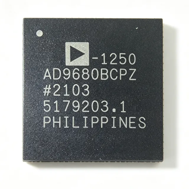
AD9680BCPZ-1250 - Dual 14-Bit 1.25 GSPS ADC JESD204B | Analog Devices
The Analog Devices AD9680BCPZ-1250 is a dual-channel, 14-bit, 1.25 GSPS pipelined analog-to-digital converter (ADC) with a JESD204B high-speed serial output interface, housed in a 64-lead LFCSP (9 mm x 9 mm) package. It is designed for sampling wide-bandwidth analog input signals of up to 2 GHz. An ADC (analog-to-digital converter) is a mixed-signal semiconductor device that converts continuous analog waveforms into discrete digital data for processing by FPGAs, DSPs, or other digital logic. Within the signal-chain hierarchy, the AD9680 belongs to the RF-sampling, high-speed pipelined ADC class, sitting upstream of digital processing elements such as the Intel/Altera and Xilinx FPGAs commonly paired with it over JESD204B serial links. Key features include dual 14-bit conversion cores running at up to 1.25 GSPS per channel, an on-chip buffer and sample-and-hold circuit optimized for low power, small size, and ease of use, and a JESD204B serial data output that dramatically reduces pin count versus parallel LVDS/CMOS interfaces. Speed-grade variants of the same family offer 500 MSPS, 820 MSPS, 1 GSPS, and 1.25 GSPS, allowing a single PCB footprint to serve multiple bandwidth tiers. Technically, the pipelined architecture uses cascaded sub-ranging stages with digital error correction, enabling high sample rates while maintaining 14-bit resolution. The integrated input buffer eases drive requirements for wideband amplifiers or passive networks, and on-chip digital functions (DDC-style processing blocks per the ADI product family) reduce FPGA resource load in digital pre-distortion and observation-receiver designs. Typical applications include wideband software-defined radios, 3G/4G/5G cellular base-station receivers, digital pre-distortion (DPD) observation channels, and test-and-measurement instrumentation requiring GHz-class analog input bandwidth. Design consideration: operate within the recommended clock and supply architecture, and budget power and thermal performance for the 64-LFCSP thermally enhanced package, since multi-gigasample operation drives the dominant portion of power dissipation. This page synthesizes distributor pricing and availability, drop-in same-family speed-grade alternatives, and practical design guidance not consolidated in the manufacturer datasheet. Pricing shown is as of 2026-09-05.
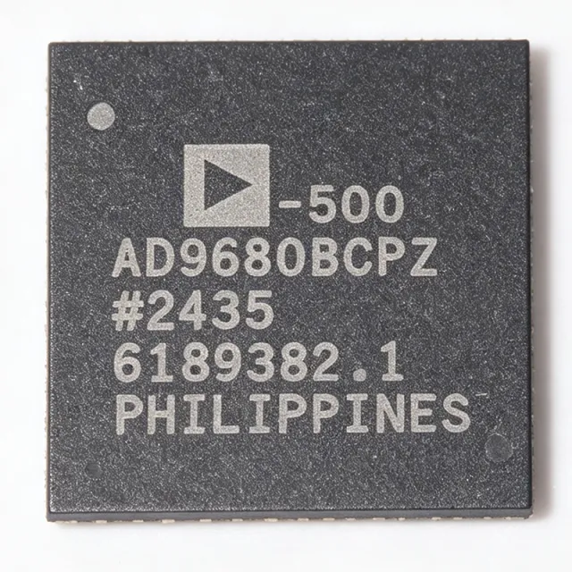
AD9680BCPZ-500 - Dual 14-Bit 500 MSPS JESD204B ADC | Analog Devices
The Analog Devices AD9680BCPZ-500 is a dual, 14-bit, 500 MSPS pipelined analog-to-digital converter (ADC) housed in a 64-lead LFCSP (9 mm x 9 mm) package with exposed pad, featuring a JESD204B serial digital output interface and 1.2 V/2.5 V dual supply operation. An analog-to-digital converter (ADC) is a mixed-signal integrated circuit that samples a continuous analog waveform and converts it into a discrete digital representation. High-speed ADCs like the AD9680 sit at the front end of the signal chain hierarchy - after amplification and filtering, and before digital processing in FPGAs or ASICs - making them critical components in any wideband data acquisition system. Key features include a 14-bit pipelined core per channel, a JESD204B high-speed serial output that drastically reduces pin count versus parallel LVDS or CMOS interfaces, an on-chip buffer and sample-and-hold circuit designed for low power, small size, and ease of use, and fast detect outputs (FD_A and FD_B on pins 17 and 32) for channel power monitoring. Architecturally, each channel uses a pipelined conversion topology in which the input is successively quantized by cascaded low-resolution stages, enabling 500 MSPS throughput while the integrated buffer relaxes external drive requirements. The multi-rail supply architecture (1.2 V core, 2.5 V analog) optimizes power consumption versus dynamic performance. Typical applications include software-defined radio and military communications receivers, wideband test and measurement instrumentation, cellular basestation receivers, and radar/electronic warfare systems where dual-channel simultaneous sampling at hundreds of megahertz is required. A key design consideration is the JESD204B link configuration and clocking architecture: a low-jitter sampling clock is essential to realize the full SNR potential of the 14-bit core, so engineers should budget jitter carefully and follow ADI reference designs for the SYSREF and device clock distribution. This page synthesizes verified distributor data, drop-in same-family alternatives, and practical engineering design guidance not found in a single manufacturer datasheet, providing a complete selection resource in one place.
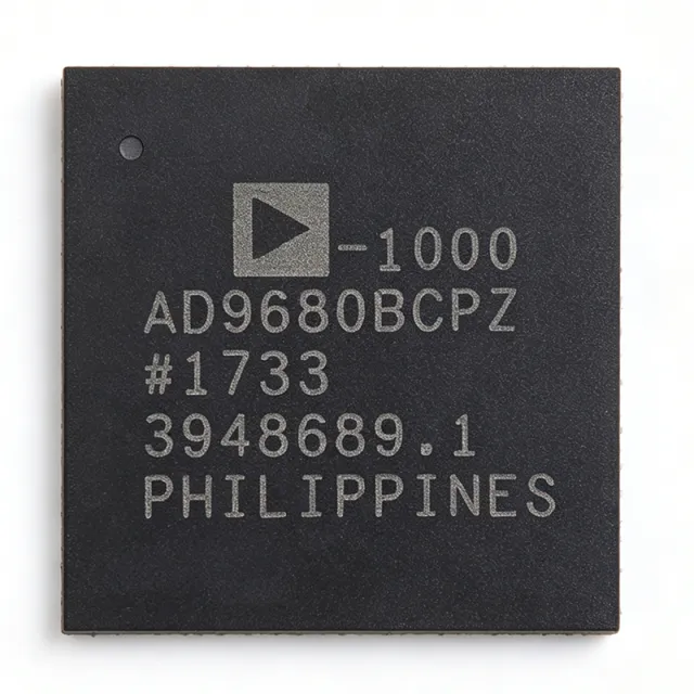
AD9680BCPZRL7-1000 - Dual 14-Bit 1 GSPS ADC JESD204B | Analog Devices
The Analog Devices AD9680BCPZRL7-1000 is a dual, 14-bit, 1 GSPS analog-to-digital converter (ADC) with a JESD204B serial data output interface, supplied in a 64-lead LFCSP (9 mm x 9 mm) package with exposed pad. An analog-to-digital converter (ADC) is a mixed-signal semiconductor that samples a continuous analog waveform and quantizes it into discrete digital values. High-speed pipelined ADCs such as the AD9680 sit at the top of the data-converter hierarchy, bridging the analog front end of an RF or IF signal chain to a digital processor, FPGA, or ASIC. In modern wideband receivers, the ADC defines the system's instantaneous bandwidth, dynamic range, and noise floor, making its selection one of the most impactful decisions in a digital receiver design. Key features of the AD9680 include dual 14-bit conversion cores rated at 1.25 GSPS (with the -1000 grade specified at 1 GSPS), an on-chip buffer and sample-and-hold circuit designed for low power, small size, and ease of use, and a JESD204B high-speed serial output that dramatically reduces pin count versus parallel LVDS/CMOS interfaces. The JESD204B lane interface supports multi-lane serialization with deterministic latency, simplifying FPGA interfacing. Architecturally, the AD9680 uses a pipelined conversion architecture with on-chip references and buffering, which minimizes external analog component count. The device operates from 1.2 V and 2.5 V supplies per the datasheet title (1.2 V/2.5 V operation), supporting low overall power consumption for its class. Multiple sampling-rate grades (1.25 GSPS / 1 GSPS / 820 MSPS / 500 MSPS) share a common register map, and ADI's SPI Controller software supports the AD9680, AD9234, and AD9690, easing design migration within the family. Typical applications include wideband software-defined radio (SDR) receivers, radar and electronic warfare digitizers, test and measurement instrumentation, and multi-channel communications infrastructure where two synchronized high-dynamic-range channels are required in a compact footprint. Design considerations: the JESD204B link requires careful FPGA-side lane mapping and sysref timing design, and the exposed-pad LFCSP package demands a well-designed thermal via array under the pad for rated performance. This page synthesizes distributor availability, same-family drop-in speed-grade alternatives, and practical design notes not found in the manufacturer datasheet alone. Pricing, where listed, is referenced as of 2026-09-05.

AD974AN - 16-Bit 4-Channel 200kSPS ADC | Analog Devices
The Analog Devices AD974AN is a four-channel, 16-bit, 200 ksps data acquisition system with a serial interface, housed in a 28-pin DIP package. It combines a four-channel input multiplexer, a successive-approximation switched-capacitor ADC, and a +2.5 V internal reference on a single chip. The device operates from one +5 V supply, supports power-down operation, and accepts analog input ranges of 0 V to +4 V, 0 V to +5 V, or ±10 V. An ADC is an analog-to-digital converter, a semiconductor that transforms continuous analog voltage signals into digital codes for processing, measurement, or transmission. The AD974 belongs to the ADC hierarchy within data-conversion ICs and power-management-dependent signal-chain components. Its four-channel multiplexer allows one 16-bit ADC core to sample multiple analog inputs sequentially, reducing board area while preserving simultaneous data-acquisition capability. Key features include 16-bit resolution, four multiplexed analog inputs, a 200 ksps conversion rate, a serial data interface, and a +2.5 V internal reference. The single +5 V supply simplifies system power architecture. Supported input ranges include 0 V to +4 V, 0 V to +5 V, and ±10 V, enabling the same converter family to serve unipolar industrial, instrumentation, and bipolar measurement systems. The AD974 uses a successive-approximation, switched-capacitor conversion architecture. This architecture is appropriate for high-resolution, moderate-speed acquisition where a serial output is sufficient and per-channel simultaneous converters would add unnecessary cost and board space. The internal +2.5 V reference supports repeatable conversion behavior without requiring a separate reference circuit, although system accuracy still depends on appropriate analog conditioning, layout, and input-range configuration. Typical applications include industrial process monitoring, sensor acquisition, laboratory measurement equipment, data logging, and embedded instrumentation. The 200 ksps sampling rate is well suited to continuously updated measurements, while 16-bit resolution supports applications requiring more detail than typical 8-bit or 12-bit converters. The four-channel input structure is particularly useful when several related signals must be scanned through a shared ADC. Designers should account for input settling time, source impedance, reference accuracy, analog noise, and the sampling interval between multiplexed channels. Place input conditioning and decoupling close to the device, preserve clean grounding around the analog pins, and verify the configured input range against the source voltage. System-level error budget should also include multiplexer transition time and any external amplifier or sensor limitations.
AD974ANZ - 4-Ch 16-Bit 200 kSPS ADC | Analog Devices
Analog Devices AD974ANZ is a four-channel, 16-bit successive-approximation data acquisition system with 200 kSPS throughput, a serial interface, and a 28-pin plastic DIP package. It operates from a single 5 V supply, supports four single-ended analog inputs, accepts 0 V to 4 V, 0 V to 5 V, or ±10 V input ranges, and includes an internal 2.5 V reference. An ADC is an analog-to-digital converter that samples continuous voltage signals and converts them into numeric values for measurement or processing. The AD974 belongs to the data acquisition system and ADC hierarchy, combining a four-channel input multiplexer, a 16-bit sampling converter, an internal reference, and a serial digital interface in one package. Its multiplexed architecture is intended for instrumentation and industrial systems that require compact multi-channel data acquisition. Key features include 16-bit resolution, 200 kSPS aggregate throughput, four single-ended input channels, and operation from one 5 V supply. A power-down function can reduce consumption from a maximum of 100 mW in the datasheet description to a typical 50 μW when the PWRD pin is asserted. The available input ranges cover unipolar 0–4 V and 0–5 V signals as well as bipolar ±10 V signals, reducing the need for separate front-end scaling circuits for different signal classes. The internal architecture uses a four-channel input multiplexer followed by a high-speed, 16-bit, successive-approximation, switched-capacitor ADC. A 2.5 V internal reference supports repeatable conversion measurements, while the serial interface provides a compact connection to a controller, DSP, or embedded data-acquisition system. The converter is designed for low-power single-supply operation and accommodates both analog and reference power-down control. Typical applications include industrial process monitoring, laboratory instrumentation, multichannel sensor acquisition, factory automation, embedded measurement systems, and compact data loggers. In each case, the four-channel multiplexer reduces the number of external analog front ends, while 200 kSPS throughput supports periodic sampling of multiple analog quantities. Systems requiring continuous simultaneous sampling rather than multiplexed acquisition need a different converter architecture. The primary design consideration is the input and reference behavior. Designers must select the correct input range, account for the maximum 120 mW power dissipation listed in the available part data, and provide suitable bypassing for the single 5 V supply. Signal conditioning may also be required to keep source impedance and voltages within the AD974 input limits. This product page consolidates the verified manufacturer specifications, distributor package information, power characteristics, and honest drop-in replacement findings. It also distinguishes verified equivalents from unsupported package variants so engineers can make a PCB-safe sourcing decision.