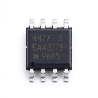
AD825AR - 30MHz High-Speed JFET Amplifier | Analog Devices
MPN: AD825AR ✓ Hoạt độngAD825AR Tóm tắt
A JFET-input operational amplifier is a voltage-amplifying semiconductor that uses junction field-effect transistors at its input. This input architecture provides low input bias current, making the AD825AR suitable for sensors, instrumentation, and high-impedance signal sources. Within the broader hierarchy, it belongs to the operational-amplifier family, which supports analog signal conditioning, measurement, feedback control, and data acquisition.
The principal advantages of the AD825AR include an input bias current of 20 pA, input voltage noise of 12 nV/sqrt(Hz), and input current noise of 10 fA/sqrt(Hz). Its 80 V/us slew rate supports accurate reproduction of rapidly changing signals, while the 30 MHz gain-bandwidth product provides useful bandwidth for low-amplitude, high-frequency content. The amplifier is optimized for fully specified ±15 V operation.
Its low-noise JFET input stage is particularly useful when source impedance makes amplifier input current important. The combination of low bias current, low voltage noise, and high slew rate allows the device to process signals from sensors, transducers, and measurement front ends without allowing input bias effects to overwhelm the wanted signal. AC performance, gain, bandwidth, slew rate, and drive capability remain stable over temperature according to the manufacturer documentation.
Typical applications include precision signal conditioning, low-level waveform acquisition, current monitoring, instrumentation, and buffered sensor interfaces. The AD825AR can also serve as an input buffer between a high-impedance transducer and a downstream measurement or conversion stage. Its operating characteristics make it particularly useful when low-frequency noise and source loading must be balanced against wideband signal support.
When designing around the AD825AR, place input and feedback components close to the relevant pins and provide adequate bypassing on the positive and negative supply rails. Confirm output swing, load current, input common-mode range, and stability requirements against the actual circuit. Avoid placing high-impedance nodes next to long switching-current paths, since parasitic capacitance can disturb gain, bandwidth, and settling behavior.
This product page combines the manufacturer specifications, a practical application analysis, same-footprint replacement guidance, and design-focused comparisons. It helps engineers evaluate the AD825AR not only by headline bandwidth, but also by noise, bias current, slew rate, drive capability, supply requirements, and PCB implementation constraints.
Bộ thay thế dễ dàng lắp đặt cho AD825AR — cùng gói, chân-to-chân tương thích. Các bộ phận yêu cầu hàn PCB bị loại trừ.
AD825ACHIPS
✅ Drop-In📋 Tham chiếu thay thế (không có trong danh mục)
AD825AR Tỷ lệ tối đa & tính chất điện
| Amplifier Type | JFET-input operational amplifier |
| Number of Channels | 1 channel |
| Gain-Bandwidth Product | 30 MHz |
| Slew Rate | 80 V/us |
| Input Bias Current | 20 pA |
| Input Voltage Noise | 12 nV/sqrt(Hz) |
| Input Current Noise | 10 fA/sqrt(Hz) |
| Fully Specified Supply Voltage | ±15 V |
| Low-Distortion Test Frequency | 1 MHz |
| Hộp | 8-lead SOIC |
| Số chân | 8 pins |
| Kiểu lắp đặt | Surface mount |
| Input Stage | JFET |
| Output Drive Capability | High output drive capability |
| Gain Stability | Stable under varying load conditions |
Cấu hình chân AD825AR
| Chân 1 | OFFSET NULL — Offset null connection |
| Chân 2 | -IN — Inverting input |
| Chân 3 | +IN — Non-inverting input |
| Chân 4 | V- — Negative supply connection |
| Chân 5 | OFFSET NULL — Offset null connection |
| Chân 6 | OUT — Amplifier output |
| Chân 7 | V+ — Positive supply connection |
| Chân 8 | NC — Not connected |
Ứng dụng tiêu biểu
AD825AR phù hợp cho 6 Áp dụngs: High-Impedance Sensor Buffering, Precision Data Acquisition Front End, Instrumentation Signal Conditioning, Current Monitoring and Measurement, Low-Level Waveform Amplification, Audio and Communication Interface Buffers.
High-Impedance Sensor Buffering
The AD825AR is appropriate for buffering high-impedance sensors because its JFET input stage has a 20 pA input bias current, reducing the current drawn from the source. A 12 nV/sqrt(Hz) input voltage noise specification also supports low-level signal conditioning. Place the amplifier near the sensor output and use short input traces to minimize capacitive loading. The 30 MHz gain-bandwidth product provides more bandwidth than is normally required for slow sensor signals, while the 80 V/us slew rate can preserve fast transients without excessive distortion.
Được đề xuất
Precision Data Acquisition Front End
AD825AR fits low-level data-acquisition front ends where input bias current and source noise determine the usable measurement floor. Its 20 pA input bias current minimizes perturbation of a high-impedance transducer, while the 12 nV/sqrt(Hz) voltage-noise figure supports precision amplification. Use it in a non-inverting or inverting conditioning stage with short feedback components. Confirm the closed-loop gain against the 30 MHz gain-bandwidth product and the 80 V/us slew rate, especially when the selected feedback resistor creates a wide bandwidth.
Được đề xuất
Instrumentation Signal Conditioning
The AD825AR can amplify instrumentation signals that combine modest bandwidth with low-level amplitude. Its JFET input architecture avoids the higher bias current associated with many bipolar input amplifiers, and the documented 20 pA value helps preserve sensor output integrity. The amplifier also offers high output drive capability for downstream instrumentation stages. Select external resistor values to establish the required gain, keep the feedback loop compact, and verify output-voltage headroom over the complete operating range before committing to the circuit.
Được đề xuất
Current Monitoring and Measurement
AD825AR is suitable for current-monitoring circuits when the sense element has appreciable source impedance and the measured waveform changes quickly. The 20 pA input bias current limits unwanted integration across a high-resistance sense path, and the 80 V/us slew rate supports clearer reproduction of rapid current edges. Use the amplifier around the sense element with attention to common-mode voltage and output swing. Its 30 MHz gain-bandwidth product makes it appropriate for small, wideband signals, but the design should still verify loop stability over the intended gain.
Được đề xuất
Low-Level Waveform Amplification
AD825AR supports low-level waveform amplification when the signal has modest amplitude but requires clean transition reproduction. The 80 V/us slew rate helps the amplifier follow changing waveforms without the slew-related distortion expected from slower devices, while the 12 nV/sqrt(Hz) input voltage noise supports small-signal work. Keep the input and feedback connections short and use grounded, stable reference connections. Check output amplitude and load capability against the measured waveform to ensure the operating point remains within the device's rated swing range.
Được đề xuất
Audio and Communication Interface Buffers
AD825AR can buffer audio or communication interface signals where low input current and moderate high-frequency performance are useful. The JFET input stage's 20 pA bias current reduces loading, and the 30 MHz gain-bandwidth product supports higher-frequency content than a conventional low-speed precision amplifier. The 80 V/us slew rate is also useful for preserving edge shapes. Use the device as a voltage follower or low-gain stage when an impedance buffer is required, and verify the source impedance, output load, and required signal bandwidth to avoid unnecessary noise or instability.
Được đề xuất
Dữ liệu tham khảo kỹ thuật cho AD825AR — so sánh, hướng dẫn thiết kế và thông tin tuân thủ.
Hướng dẫn chọn lựa
So sánh với các sản phẩm thay thế
| Tham số | Sản phẩm này | AD825ACHIPS |
|---|---|---|
| Brand | Analog Devices | Analog Devices |
| Package | 8-SOIC | 8-SOIC |
| Gain-Bandwidth Product | 30 MHz | 26 MHz |
| Common-Mode Rejection Ratio | 80 dB | 80 dB |
| Number of Channels | 1 channel | 1 channel |
Bảo phân biệt quan trọng
- Higher published gain-bandwidth product within the AD825 family (vsAD825ACHIPS)
- JFET input architecture for low source loading (vsAD825ACHIPS)
- Low-noise input characterized for precision conditioning (vsAD825ACHIPS)
Ghi chú thiết kế
Place input, feedback, and bypass components close to their corresponding AD825AR pins. High-impedance input traces should be short and surrounded by a grounded reference plane where practical. Keep the inverting-input and feedback nodes compact because parasitic capacitance in the feedback loop can alter bandwidth and stability. Follow the manufacturer datasheet's pin configuration and printed-circuit-board layout guidance for the 8-lead SOIC footprint.
Use local supply bypassing to control impedance on the V+ and V- pins, and route the return current through a low-impedance path rather than through analog-signal ground. Decoupling capacitance and placement should be selected with the actual source impedance and expected transient load in mind. Verify that both supply rails remain within the limits specified by the AD825 datasheet under startup, shutdown, and load transients.
The AD825AR's 30 MHz gain-bandwidth product and 80 V/us slew rate make input capacitance and excess loop gain important at higher frequencies. Select feedback resistors that preserve the intended bandwidth and avoid unnecessarily large resistance at the inverting input. Confirm output loading and amplitude before assuming the full small-signal bandwidth or slew-rate capability is usable in the finished circuit.
Do not select a replacement based only on the JFET label or bandwidth. Check pinout, package dimensions, input bias current, voltage noise, common-mode range, output swing, supply requirements, and stability together. AD825ACHIPS is a related family option, but its published 26 MHz gain-bandwidth product is lower than the AD825AR's 30 MHz value. Verify the exact ordering code before treating it as interchangeable.
Thông tin tuân thủ
Compliance status was not established for the exact AD825AR ordering code and requires review of the current manufacturer environmental and material declarations.