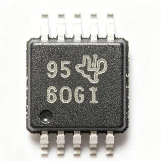
ADS801U - 12-Bit 25-MSPS ADC | Texas Instruments
MPN: ADS801U ✓ Hoạt độngADS801U Tóm tắt
An ADC is a data-converter category that samples an analog voltage and converts it into a digital code for processing, storage, display, or control. The ADS801U belongs to the parallel-output pipelined ADC family and is positioned between general-purpose mixed-signal processing and high-speed measurement. Its 12-bit resolution provides 4096 quantization levels, while the 25-MSPS sampling rate supports rapidly changing signals when the analog front end and system clock are designed appropriately.
Key features include no missing codes, a 65 MHz track-and-hold bandwidth, internal references, single-ended or differential input configuration, and compatibility with ADS800 and ADS802 pin arrangements. The single +5 V supply simplifies system power design, while the three-state outputs support bus-oriented connection to digital logic. The supplied technical data identifies a 54 mA supply current and an industrial temperature grade of -40 °C to +85 °C for the ADS801U package.
The converter uses a small-geometry CMOS process and a pipelined conversion architecture. Pipelining supports high throughput by dividing the conversion process into stages, although system designers must account for the device's specified acquisition and conversion timing. The 28-pin SOIC package is intended for surface-mount assembly and includes analog, digital, reference, and control connections.
Typical applications include industrial measurement, communications equipment, test and measurement instrumentation, control systems, and embedded signal acquisition. The 25 MSPS rate is useful when sampling waveforms or feedback signals, while 12-bit resolution balances data fidelity against digital interface bandwidth. Differential input support can improve signal integrity when the source is balanced and the PCB layout is controlled.
Designers should verify the exact pinout, analog input range, reference configuration, timing, output coding, and package details in the manufacturer datasheet before layout. Keep analog and digital return paths separated, place bypass capacitance near the supply pins, and provide a controlled input source. The SOIC footprint also allows easy breadboard and prototype assembly, although production layouts should minimize parasitic capacitance and digital crosstalk.
Bộ thay thế dễ dàng lắp đặt cho ADS801U — cùng gói, chân-to-chân tương thích. Các bộ phận yêu cầu hàn PCB bị loại trừ.
Các biến thể trong loạt này
Các mẫu cùng loạt có thể lắp đặt dễ dàng tương thích với ADS801U (cùng hình factor và footprint) — khác nhau ở Package, Process Technology.
ADS802U
✅ Drop-InLiên hệ để biết giá
Xem tài liệu →ADS801UG4
✅ Drop-In📋 Tham chiếu thay thế (không có trong danh mục)
ADS801U Tỷ lệ tối đa & tính chất điện
| Không có thông số kỹ thuật sẵn có |
Hướng dẫn cấu hình chân ADS801U standard
Cấu hình chân cho ADS801U (standard gói). Thành phần số hiệu này có chân đầu vào, đầu ra và nguồn cung cấp. Tham khảo tài liệu thông số kỹ thuật của nhà sản xuất để biết cấu hình chân bù, bù trừ và chân kích hoạt. Hoàn hảo cho điều kiện tín hiệu và mạch khuếch đại.

Không có dữ liệu chân cụ thể sẵn có cho ADS801U.
Tham khảo: tài liệu kỹ thuật cho cấu hình chân đầy đủ.
Ứng dụng tiêu biểu
ADS801U phù hợp cho 6 Áp dụngs: Industrial Signal Acquisition, Test and Measurement Instrumentation, Communications and Control Loops, Waveform Monitoring, Sensor Interface Systems, Embedded Data Acquisition.
Industrial Signal Acquisition
ADS801U fits industrial signal-acquisition systems that need a compact 12-bit converter with a 25 MSPS sampling rate. The 65 MHz track-and-hold bandwidth gives the analog front end useful bandwidth margin for conditioning sensor or process signals. Its single +5 V supply simplifies system integration, while single-ended or differential input selection allows the board to support grounded sensors or balanced sources. Designers should place the converter close to the input network, use stable bypass capacitors, and verify the acquisition timing for the required waveform bandwidth.
Được đề xuất
Test and Measurement Instrumentation
ADS801U is appropriate for oscilloscope-like, instrumentation, and automated test systems that sample waveforms at up to 25 MSPS. The 12-bit quantizer provides 4096 digital codes, offering a practical balance between resolution, data rate, and parallel-output implementation. Its three-state outputs can simplify connection to digital acquisition logic when the surrounding bus architecture supports them. The analog input path still needs sufficient bandwidth, low noise, controlled grounding, and calibration to achieve useful measurement accuracy.
Được đề xuất
Communications and Control Loops
ADS801U can serve as the sampling element in communications equipment and control systems that monitor rapidly varying analog feedback. Its 25 MSPS rate supports higher throughput than lower-speed general-purpose converters, while differential input support can help reject common-mode noise on balanced signals. The design must still account for digital clock routing, output timing, input bandwidth, and system latency. For closed-loop control, verify whether the application needs simultaneous sampling or other features not specified in the verified data.
Được đề xuất
Waveform Monitoring
ADS801U is suitable for waveform monitoring when the sampled signal is within the converter's input and bandwidth requirements. The 65 MHz track-and-hold bandwidth supports acquisition of higher-frequency content than the 25 MSPS sampling rate alone might imply, although anti-aliasing and output timing must be designed correctly. Differential input can be valuable in noisy environments, while single-ended input can simplify lower-cost sensor interfaces. Digital storage and processing should account for the parallel output timing and acquisition latency.
Được đề xuất
Sensor Interface Systems
ADS801U can convert conditioned outputs from pressure, position, current, and other analog sensors when the required bandwidth justifies a 25 MSPS converter. A single-ended input simplifies single-supply sensor interfaces, while differential input can reduce sensitivity to common-mode voltage in balanced circuits. The internal reference and integrated track-and-hold reduce the number of separate blocks needed for a compact acquisition channel. Calibration, input scaling, grounding, and protection must be added externally because those functions are not fully specified in the verified data.
Được đề xuất
Embedded Data Acquisition
ADS801U is appropriate for an embedded acquisition module when the host processor can receive parallel digital samples and the application needs more sampling capability than a slow integrated ADC. The 28-pin SOIC package is convenient for prototype boards and conventional surface-mount assembly, while the 12-bit output provides a straightforward digital interface. Because the verified material does not specify all timing and logic-level details, the host interface should be designed only after checking the current manufacturer datasheet and validating output timing.
Được đề xuất
Tóm tắt các sản phẩm được đề xuất
Dữ liệu tham khảo kỹ thuật cho ADS801U — so sánh, hướng dẫn thiết kế và thông tin tuân thủ.
Hướng dẫn chọn lựa
So sánh với các sản phẩm thay thế
| Tham số | Sản phẩm này | ADS802U | ADS801UG4 |
|---|---|---|---|
| Brand | Texas Instruments | Texas Instruments | Texas Instruments |
| Package | 28-pin SOIC (DW) | 28-pin SOIC (DW), reported pin-compatible | SOIC-28 |
Bảo phân biệt quan trọng
- Higher sampling rate than the verified TI replacement candidate (vsADS802U)
- Explicit 12-bit quantization (vsADS802U)
- Wideband track-and-hold capability (vsADS802U)
- Single +5 V operation (vsADS801UG4)
Ghi chú thiết kế
Route analog input and reference connections away from digital output and clock traces. Keep the ADC input network close to the converter, use a continuous ground reference, and place supply bypass capacitance near the +5 V and ground pins. Because ADS801U is a high-speed converter, uncontrolled trace inductance and parasitic capacitance can degrade acquisition behavior even when the nominal sampling rate is within specification.
Verify acquisition and conversion timing with the current manufacturer datasheet before setting the sampling clock. The converter's 25 MSPS rating and 65 MHz track-and-hold bandwidth do not guarantee usable performance for every input frequency. Account for source impedance, amplifier settling time, anti-alias filtering, and clock jitter so that the analog front end can settle before each sample.
Do not substitute ADS802U without checking throughput. The verified TI support result identifies ADS802U as a drop-in replacement candidate, but its 10 MHz sampling frequency is substantially below ADS801U's 25 MHz. It may be usable in lower-bandwidth designs, yet it can change system timing and bandwidth behavior. Confirm package pinout, input range, timing, and output coding against the current datasheet.
For differential inputs, route the signal pair with matched geometry and controlled return paths, and keep the analog and digital grounds arranged to minimize shared impedance. The verified data confirms differential input support, but it does not provide the complete recommended layout or input-range values. Those details must be obtained from the official ADS801 datasheet before high-speed board release.
Thông tin tuân thủ
The verified search results identify the industrial -40 °C to +85 °C temperature grade but do not provide explicit RoHS, REACH, lead-free, halogen-free, conflict-minerals, or AEC-Q100 statements. ADS801U is an analog-to-digital converter rather than an automotive-qualified device in the supplied data.