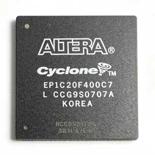
EP1C20F400C6AB - 20K LE Cyclone FPGA, 301 I/O, 400-FBGA | Intel
MPN: EP1C20F400C6AB ✗ Cuối đờiEP1C20F400C6AB Tóm tắt
A Field Programmable Gate Array (FPGA) is a programmable semiconductor that implements custom digital logic via a configurable array of logic elements (LEs), embedded memory blocks, multiplier blocks, and programmable I/O cells surrounding a routing fabric. FPGAs occupy the middle ground between fixed-function ASICs and software-driven microcontrollers: faster and more parallel than an MCU for datapath and glue-logic workloads, but reprogrammable and lower-NRE than an ASIC. The Cyclone family sits at the low-cost / low-power end of the FPGA hierarchy (Cyclone -> low-cost FPGA -> programmable logic -> semiconductor) and is widely deployed in consumer, industrial, communications, and prototyping designs.
Key features of the EP1C20F400C6AB include 20,060 logic elements, 288 Kbits (36 Kbits x 8) of M4K embedded memory blocks, up to 200 MHz internal operation, LVDS support on selected I/O banks, a dedicated PLL for clock conditioning, and 301 user I/O pins with multi-standard I/O support (LVTTL, LVCMOS, SSTL, HSTL). The device is configured via an industry-standard serial configuration device such as the EPCS4 or EPCS16, enabling fast in-system reconfiguration.
The EP1C20F400C6AB utilizes a 0.13-µm SRAM-based LUT architecture with embedded M4K RAM blocks and multiplier blocks distributed across the fabric. Each logic element contains a 4-input lookup table, a programmable flip-flop, and dedicated carry-chain logic, allowing efficient implementation of arithmetic, state machines, and bus interfaces while sustaining high performance on signal-processing pipelines.
Typical applications include industrial control and factory-automation backplanes, video/image processing front-ends, communications line-card glue logic, consumer-electronics display controllers, ASIC prototyping, and PCI/PCI-X bridge designs. The 400-FBGA FineLine BGA package supports high I/O density while keeping the board footprint manageable for multi-layer PCBs.
Designers should plan for a clean, multi-layer PCB with continuous power planes for VCCINT (1.5 V) and VCCIO (per-bank), proper decoupling near every VCC/VCCIO/VCCPD pin, and a series-termination strategy for high-speed LVDS or SSTL signaling. Configuration mode (AS, PS, JTAG) and the EPCS serial-configuration flash selection must be finalized before layout to avoid board rework.
This page synthesizes distributor stock, package-level alternatives, and practical design notes that go beyond the manufacturer datasheet to accelerate component selection and BOM risk reduction.
Bộ thay thế dễ dàng lắp đặt cho EP1C20F400C6AB — cùng gói, chân-to-chân tương thích. Các bộ phận yêu cầu hàn PCB bị loại trừ.
Các biến thể trong loạt này
Các mẫu cùng loạt có thể lắp đặt dễ dàng tương thích với EP1C20F400C6AB (cùng hình factor và footprint) — khác nhau ở Package, Speed Grade, Operating Temperature, Process Technology, Total RAM Bits.
EP1C20F400C6N
✅ Drop-InLiên hệ để biết giá
Xem tài liệu →EP1C20F400
✅ Drop-InLiên hệ để biết giá
Xem tài liệu →EP1C20F40017
✅ Drop-InLiên hệ để biết giá
Xem tài liệu →EP1C12F400I7N
✅ Drop-In ⚠️ Thông số chưa được xác minh📋 Tham chiếu thay thế (không có trong danh mục)
EP1C20F324C6N
✅ Drop-In ⚠️ Thông số chưa được xác minhLiên hệ để biết giá
Xem tài liệu →EP1C20F400C6AB Tỷ lệ tối đa & tính chất điện
| Family | Cyclone |
| Logic Elements | 20,060 |
| User I/O Pins | 301 |
| Embedded Memory Bits | 294,912 bits |
| Embedded Memory Blocks | M4K, 36 Kbits each (8 blocks typical family-wide) |
| Hộp | 400-ball FineLine BGA (FBGA-400) |
| Process Technology | 0.13 µm SRAM |
| Core Voltage (VCCINT) | 1.5 V |
| Nhiệt độ hoạt động | 0°C to 85°C (commercial) |
| Speed Grade | C6 |
| Maximum User I/O | 301 |
| Configuration Mode | Active Serial (AS), Passive Serial (PS), JTAG |
| PLLs | 2 (per Cyclone family datasheet) |
| Kiểu lắp đặt | Surface Mount (BGA) |
Hướng dẫn cấu hình chân EP1C20F400C6AB 400-ball fineline bga (fbga-400)
Cấu hình chân cho EP1C20F400C6AB (400-ball fineline bga (fbga-400) gói). IC số này bao gồm chân GPIO, giao diện truyền thông (UART, SPI, I2C) và chân nguồn. Tham khảo tài liệu thông số kỹ thuật của nhà sản xuất để biết các chức năng chân thay thế và tùy chọn cấu hình. Cực kỳ quan trọng cho thiết kế hệ thống tích hợp và lập trình PCB.

Không có dữ liệu chân cụ thể sẵn có cho EP1C20F400C6AB.
Tham khảo: tài liệu kỹ thuật cho cấu hình chân đầy đủ.
Ứng dụng tiêu biểu
EP1C20F400C6AB phù hợp cho 6 Áp dụngs: Industrial Control and Factory Automation, ASIC Prototyping and Emulation, Video and Image Processing Front-End, Communications Line-Card Glue Logic, Consumer Electronics Display Controller, PCI / PCI-X Bridge and I/O Expansion.
Industrial Control and Factory Automation
The EP1C20F400C6AB fits industrial control backplanes where multiple sensors, actuators, and communication buses must be aggregated and processed in parallel. Its 20,060 logic elements provide enough capacity to implement custom Profibus, Modbus, or EtherCAT slave interfaces alongside motor-control state machines, while the 301 user I/O pins fan out to dozens of optoisolated digital lines. The 1.5 V VCCINT core and commercial 0°C to 85°C temperature grade suit IP20/IP54 control cabinets. Designers typically pair the FPGA with an EPCS16 configuration flash and an external SRAM bank for data logging. Trade-off: the legacy Cyclone fabric draws more power per LE than Cyclone IV E, so total board power dissipation may exceed newer designs.
Được đề xuất
ASIC Prototyping and Emulation
Designers use the EP1C20F400C6AB to prototype and validate mid-complexity ASICs before tape-out, where 20,060 LEs can map a working subset of the target ASIC. The M4K RAM blocks (294 Kbits total) emulate internal ASIC register files and FIFOs, while the 301 I/O pins map to ASIC pads via level-shifters. Quartus II software synthesizes Verilog or VHDL into the FPGA, allowing real-time functional verification at 50-100 MHz, well below ASIC speeds but sufficient for logic and protocol verification. The 400-FBGA package supports the high I/O density typical of pad-limited ASICs. Note: legacy Quartus II versions (8.0 to 13.0) are required for this device family.
Được đề xuất
Video and Image Processing Front-End
The EP1C20F400C6AB is well matched to mid-resolution video pre-processing such as scaling, color-space conversion, and de-interlacing. Its M4K RAM blocks can buffer 720p video lines (each M4K block holds 4 Kbits, enough for short pixel FIFOs), while the 200 MHz fabric supports pixel-rate processing at 27 MHz for standard-definition and 74.25 MHz for 720p HD-SDI. The LVDS-capable I/O banks connect directly to LVDS deserializer chips. Use the PLL to derive pixel clocks from the incoming video reference. Limitation: hard DSP/multiplier blocks are limited, so heavy FIR filtering is more efficient on Cyclone II or later families.
Được đề xuất
Communications Line-Card Glue Logic
Telecom line cards use the EP1C20F400C6AB to bridge backplane buses, implement proprietary framing, and provide parallel protocol translation between TDM, UART, and SPI peripherals. The 301 user I/O pins accommodate dozens of LVCMOS and HSTL bus lines typical of telecom backplanes, while the 2 PLLs synthesize multiple clock frequencies from a single backplane reference. The M4K RAM blocks store framing buffers and elastic FIFOs for clock-domain crossing. Although the part is obsolete, long-life telecom customers continue to use it in legacy line cards, often sourcing from authorized distributors with full traceability.
Được đề xuất
Consumer Electronics Display Controller
Consumer display controllers and digital signage players use the EP1C20F400C6AB to implement custom timing controllers (TCONs) for LCD panels, HDMI-to-LVDS bridges, and LED matrix drivers. The high I/O count supports multi-lane LVDS interfaces to large LCD panels, while the logic capacity accommodates frame-rate conversion and overdrive algorithms. The 1.5 V core and 400-FBGA package keep the design small enough for slim display enclosures. Designers must verify the long-term availability of this obsolete part with procurement; otherwise migrate to Cyclone IV E or Cyclone 10 LP with a fresh pin-migration report.
Được đề xuất
PCI / PCI-X Bridge and I/O Expansion
The EP1C20F400C6AB implements PCI 32-bit / 33 MHz target or master interfaces plus custom local-bus expansion for legacy peripheral cards. The 301 user I/O pins comfortably host a 32-bit PCI bus plus 32 to 64 local-bits, while the 2 PLLs generate the 33 MHz PCI clock from a backplane reference. The M4K blocks buffer FIFO elasticity between PCI and local bus clocks. Quartus II includes the altpci megafunction, which synthesizes the full PCI target interface in under 2000 LEs, leaving room for application logic. Industrial and instrumentation customers commonly deploy this part in test-and-measurement chassis.
Được đề xuất
Tóm tắt các sản phẩm được đề xuất
Dữ liệu tham khảo kỹ thuật cho EP1C20F400C6AB — so sánh, hướng dẫn thiết kế và thông tin tuân thủ.
Hướng dẫn chọn lựa
So sánh với các sản phẩm thay thế
| Tham số | Sản phẩm này | EP1C20F400C6N | EP1C20F400 | EP1C20F40017 | EP1C12F400I7N |
|---|---|---|---|---|---|
| Package | 400-ball FineLine BGA | 400-ball FineLine BGA - same | 400-ball FineLine BGA - same | 400-ball FineLine BGA - same | 400-ball FineLine BGA - same |
| Brand | Intel | Intel | Intel | Intel | Intel |
| Logic Elements | 20,060 | 20,060 | 20,060 | 20,060 | 12,060 |
| Embedded Memory | 294,912 bits | 294,912 bits | 294,912 bits | 294,912 bits | 239,616 bits |
| User I/O Pins | 301 | 301 | 301 | 301 | 301 |
| Operating Temperature | 0°C to 85°C (commercial) | 0°C to 85°C (commercial) | 0°C to 85°C (commercial) | 0°C to 85°C (commercial) | -40°C to 100°C (industrial) |
| Speed Grade | C6 | C6 | C6 default | C6 | I7 |
| Lead-Free Finish | AB finish (per Intel/Altera convention) | Lead-free | Varies | Varies | Lead-free |
Bảo phân biệt quan trọng
- Highest logic-element density in the original Cyclone family with 400-FBGA I/O (vsEP1C12F400I7N)
- Commercial temperature range versus industrial on smaller Cyclone variants (vsEP1C12F400I7N)
- Cyclone-20 silicon versus Cyclone II silicon (vsEP2C20F400C7N)
Ghi chú thiết kế
The EP1C20F400C6AB requires two independent power rails: VCCINT at 1.5 V (core logic, roughly 30 mA static per 1000 LEs) and VCCIO per I/O bank at 1.5/1.8/2.5/3.3 V. Decouple each VCCINT/VCCIO pin with a 0.1 µF X7R ceramic placed within 100 mils, and add a bulk 47 µF tantalum per supply zone. A clean VCCAUX at 2.5 V is required for the PLL and JTAG circuitry; tie it up before VCCINT during power sequencing to avoid latch-up. Estimated: at full 20K-LE utilization with all I/O toggling, total board power is approximately 1.5 to 2.0 W, well within the FBGA-400 thermal envelope.
The 400-ball FineLine BGA uses 1.0 mm ball pitch; escape routing requires a minimum 4-layer PCB with a dedicated ground plane on layer 2 directly under the BGA. Use microvias (laser-drilled, 0.1 mm pad) for the inner rows; the outermost 2 rows can be routed with 0.15 mm trace-and-space on conventional FR-4. Add 4 to 8 thermal vias in a 3x3 grid under the central ground balls for heat dissipation. All configuration pins (MSEL, nCONFIG, nSTATUS, CONF_DONE) must be pulled to their idle levels per the Cyclone family datasheet configuration scheme.
Do not apply VCCINT before VCCAUX during power-up; Cyclone-family SRAM FPGAs can experience partial configuration and high inrush current if sequencing is wrong. Always include a JTAG header (TCK, TMS, TDI, TDO, plus GND and VCCIO pull-ups) for in-system programming and board bring-up. The Cyclone-20 device is supported by Quartus II versions 2.1 through 13.0sp1 only; do not attempt to load bitstreams generated by Quartus Prime 18+ because the configuration bitstream format is incompatible.
Thông tin tuân thủ
Compliance data not provided in the verified web data; AB finish suffix historically indicates Pb-free but the manufacturer page should be confirmed for current RoHS/REACH status.