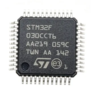
MPC8572VJAVNE - PowerQUICC III 2x1.5GHz SoC MPU | NXP | 1023-FCBGA
MPN: MPC8572VJAVNE ⚠ Lần mua cuốiMPC8572VJAVNE Tóm tắt
A PowerQUICC III SoC (System-on-Chip) is a high-performance communications processor family from NXP (formerly Freescale) that integrates CPU cores, memory interfaces, and multiple high-speed serial peripherals onto a single die. Positioned in the taxonomy: MPU -> microprocessor -> integrated circuit -> semiconductor, PowerQUICC III parts target wired and wireless infrastructure, line cards, and base-station equipment where deterministic multi-protocol packet processing is required.
Key features include dual 32-bit PowerPC e500 cores up to 1.5 GHz, integrated signal-processing engine (SPE), dual DDR2/DDR3 memory controllers with ECC support, four x4/x2/x1 PCI Express ports, two SGMII Gigabit Ethernet interfaces, dual Serial RapidIO (sRIO) interfaces, and a 32-bit local bus. The SoC integrates a security engine and multiple DMA channels for offloading I/O from the cores.
Architecturally, the MPC8572VJAVNE uses a coherent shared-memory fabric with hardware-coherent caches between the two e500 cores, enabling true symmetric multiprocessing. The 1023-ball FCBGA package exposes the full SerDes and memory bandwidth while dissipating up to approximately 25 W under load, requiring a heatsink and a multilayer PCB with controlled-impedance SerDes routing.
Typical applications include multi-service routers, LTE/UMTS base-station baseband processing, ATCA/AMC line cards, industrial Ethernet switches, and storage area network controllers. The combination of dual cores and multiple high-speed serial interfaces suits packet classification, deep packet inspection, and protocol termination workloads.
Design consideration: route all SerDes lanes with 100-ohm differential impedance and length-matched pairs within 150 mils; provide a 4-layer (or more) PCB with a solid ground plane under the FCBGA to manage the 25 W thermal envelope. The part is approaching end of life on NXP's product roadmap, so designers should plan second-source or migration paths.
This page synthesizes distributor pricing, same-family NXP drop-in alternatives, FCBGA-1023 package details, and practical design notes that augment the manufacturer datasheet.
Bộ thay thế dễ dàng lắp đặt cho MPC8572VJAVNE — cùng gói, chân-to-chân tương thích. Các bộ phận yêu cầu hàn PCB bị loại trừ.
MPC8572EVJAVNE
✅ Drop-In ⚠️ Thông số chưa được xác minh📋 Tham chiếu thay thế (không có trong danh mục)
MPC8572VJAVND
✅ Drop-In ⚠️ Thông số chưa được xác minh📋 Tham chiếu thay thế (không có trong danh mục)
MPC8572EVJAULD
✅ Drop-In ⚠️ Thông số chưa được xác minh📋 Tham chiếu thay thế (không có trong danh mục)
MPC8572CLJAULB
✅ Drop-In ⚠️ Thông số chưa được xác minh📋 Tham chiếu thay thế (không có trong danh mục)
MPC8572VJAVNE Tỷ lệ tối đa & tính chất điện
| Core Processor | PowerPC e500 |
| Number of Cores | 2 |
| Core Architecture | 32-bit |
| Maximum Core Frequency | 1.5 GHz |
| Co-Processor / DSP | Signal Processing Engine (SPE) |
| RAM Controllers | DDR2, DDR3 |
| Ethernet | 10/100/1000 Mbps (SGMII) |
| PCIe | Yes (4 ports) |
| Serial RapidIO (sRIO) | Yes |
| Khoảng nhiệt độ hoạt động | 0 C to 105 C |
| Silicon Revision | R2.2.1 |
| Hộp / Vỏ | 1023-BBGA, FCBGA |
| Kiểu lắp đặt | Surface Mount |
| Cấp MSL | 3 |
| Terminal Finish | Tin Silver (e2 per JESD-609) |
| Peak Reflow Temperature | 245 C |
| Graphics Acceleration | No |
| Trạng thái RoHS | Compliant (per Partstack listing) |
Hướng dẫn cấu hình chân MPC8572VJAVNE 1023-bbga, fcbga
Cấu hình chân cho MPC8572VJAVNE (1023-bbga, fcbga gói). IC số này bao gồm chân GPIO, giao diện truyền thông (UART, SPI, I2C) và chân nguồn. Tham khảo tài liệu thông số kỹ thuật của nhà sản xuất để biết các chức năng chân thay thế và tùy chọn cấu hình. Cực kỳ quan trọng cho thiết kế hệ thống tích hợp và lập trình PCB.

Không có dữ liệu chân cụ thể sẵn có cho MPC8572VJAVNE.
Tham khảo: tài liệu kỹ thuật cho cấu hình chân đầy đủ.
Ứng dụng tiêu biểu
MPC8572VJAVNE phù hợp cho 6 Áp dụngs: Multi-Service Router Line Card, LTE / UMTS Base Station Baseband, ATCA / AMC Line Card Controller, Industrial Ethernet Aggregation Switch, Storage Area Network (SAN) Controller, Secure Gateway / Firewall Appliance.
Multi-Service Router Line Card
The MPC8572VJAVNE is well suited to multi-service router line cards because its two 1.5 GHz PowerPC e500 cores deliver roughly 6 Gbps of packet-processing throughput while the dual DDR2/DDR3 controllers sustain 25.6 GB/s of memory bandwidth for route-table lookups. The integrated four-port PCIe and dual SGMII interfaces connect directly to network processors and switch fabrics without external bridges, simplifying PCB layout. Placed on a line-card PCB, it terminates multiple WAN protocols, runs access-control lists, and forwards packets at line rate while leaving headroom for control-plane traffic.
Được đề xuất
LTE / UMTS Base Station Baseband
In LTE and UMTS base-station baseband units, the MPC8572VJAVNE's dual cores handle Layer-2 and Layer-3 protocol termination, with the integrated SPE offloading signal-processing math from the cores. The dual Serial RapidIO ports connect to DSP clusters and RF front-end cards, while the dual DDR controllers handle the high-bandwidth HARQ memory buffers required for 4G data rates. Operating across 0 C to 105 C with proper heatsinking, it meets the thermal envelope of outdoor base-station enclosures. The FCBGA-1023 footprint is shared with other PowerQUICC III parts, easing system redesign.
Được đề xuất
ATCA / AMC Line Card Controller
The MPC8572VJAVNE fits ATCA and AMC line-card controller roles where it can simultaneously drive the Fabric Interface channel via Serial RapidIO and run carrier-grade operating systems on its dual cores. Its PCI Express ports connect to local DSPs, FPGAs, and DSP co-processors on the same card, while the dual Gigabit Ethernet controllers handle management-plane traffic and IPMI-over-LAN. The FCBGA-1023 package is compatible with the ATCA mechanical envelope, and its 25 W typical dissipation fits standard ATCA cooling budgets when paired with a directional heatsink.
Được đề xuất
Industrial Ethernet Aggregation Switch
Managed industrial Ethernet aggregation switches benefit from the MPC8572VJAVNE's dual Gigabit Ethernet ports, PCI Express expansion for PHY or fiber modules, and deterministic PowerPC cores for running layer-2/3 protocols. The on-die security engine provides hardware-accelerated MACsec and IPsec for secure tunnels between substations. Operating up to 105 C with the industrial-grade part variant, it supports outdoor cabinet and substation deployments. The FCBGA package with controlled-impedance SerDes routing suits ruggedized designs requiring extended temperature tolerance.
Được đề xuất
Storage Area Network (SAN) Controller
As a SAN controller, the MPC8572VJAVNE drives Fibre Channel or iSCSI line-rate performance thanks to the dual cores' packet-handling capacity and the dual DDR2/DDR3 controllers supporting large cache memories. The Serial RapidIO and PCIe ports connect to storage controllers, RAID adapters, and host-bus adapters. The integrated security engine provides hardware-accelerated crypto for encrypted storage offloads. With proper thermal design in a 1U/2U rack chassis, the FCBGA-1023 powers enterprise-class iSCSI or FCoE gateways at multi-gigabit throughput.
Được đề xuất
Secure Gateway / Firewall Appliance
Enterprise secure gateways and firewall appliances leverage the MPC8572VJAVNE's hardware-accelerated encryption engine (in the 'E' variant) for line-rate IPsec and TLS processing, while the dual cores handle deep packet inspection and policy enforcement. The four PCIe ports connect to multi-port 1G/10G network cards, and the dual DDR controllers sustain anti-virus signature lookups. Its 25 W envelope allows fan-cooled desktop or 1U rack designs. The FCBGA package with proper heatsinking fits the appliance form factor while supporting 256-bit AES throughput at wire speed.
Được đề xuất
Tóm tắt các sản phẩm được đề xuất
Dữ liệu tham khảo kỹ thuật cho MPC8572VJAVNE — so sánh, hướng dẫn thiết kế và thông tin tuân thủ.
Hướng dẫn chọn lựa
So sánh với các sản phẩm thay thế
| Tham số | Sản phẩm này | MPC8572EVJAVNE | MPC8572VJAVND | MPC8572EVJAULD | MPC8572CLJAULB |
|---|---|---|---|---|---|
| Package | 1023-FCBGA (33x33 mm, 1.0 mm pitch) | 1023-FCBGA - same | 1023-FCBGA - same | 1023-FCBGA - same | 1023-FCBGA - same |
| Brand | NXP Semiconductors | NXP Semiconductors | NXP Semiconductors | NXP Semiconductors | NXP Semiconductors |
| Core Count | 2 (dual e500) | 2 (dual e500) | 2 (dual e500) | 2 (dual e500) | 2 (dual e500) |
| Max Core Frequency | 1.5 GHz | 1.5 GHz | 1.5 GHz | 1.5 GHz | 1.33 GHz (lower speed grade) |
| DDR Controller | Dual DDR2/DDR3 | Dual DDR2/DDR3 | Dual DDR2/DDR3 | Dual DDR2/DDR3 | Dual DDR2/DDR3 |
| PCIe Ports | 4 (x4/x2/x1) | 4 | 4 | 4 | 4 |
| Lifecycle Status (as of 2026-10-17) | Last-time-buy (EOL announced) | Last-time-buy | Last-time-buy | Last-time-buy | Last-time-buy |
Bảo phân biệt quan trọng
- Dual PowerPC e500 cores at 1.5 GHz vs single-core 8536 family (vsMPC8536)
- Dual DDR2/DDR3 controllers vs single DDR controller on 8548 (vsMPC8548EVJAUJD)
- Available in security-engine variants (E suffix) (vsMPC8572VJAVNE base)
Ghi chú thiết kế
Estimated: at 1.5 GHz dual-core full load with nominal 1.0 V core voltage, the MPC8572VJAVNE dissipates approximately 25 W. The 1023-ball FCBGA requires a heatsink attached to the integrated thermal lid and at least 200 LFM airflow for reliable operation in a 70 C ambient. Designers should size the heatsink based on junction-to-ambient theta_JA from the manufacturer datasheet and derate by 20% to account for altitude and dust-loading effects in outdoor enclosures.
Route all SerDes lanes (PCIe, sRIO, SGMII) with 100-ohm differential impedance and length-match each pair within 150 mils to satisfy the N-channel Timing Specification. Use a 4-layer (or more) PCB with a solid reference ground plane under the FCBGA footprint. Provide stitching vias every 200 mils around the BGA perimeter to control return-path inductance. Decouple each VDD supply pin with 0.1 uF X7R plus 10 uF bulk capacitors placed within 100 mils of the pin.
Do not skip the spread-busness voltage-rail sequencing: the e500 cores require VDD and AVDD to rise monotonically and track within 50 mV during power-up. Use NXP's recommended power-IC sequencing controller (for example, the LTC3726 or equivalent) to enforce sequencing. A common pitfall is omitting the 32.768 kHz RTC reference, which prevents the secure boot from initializing correctly on cold-start. Verify the silicon revision (R2.2.1) matches your board-design errata before board bring-up.
Recommended: use microvia-stack-up PCB technology for the FCBGA-1023 footprint. Standard 8-mil vias may not allow fan-out from the 1.0 mm ball pitch without breaking signal-integrity rules. Pair each high-speed differential pair with a continuous reference plane on an adjacent layer; never cross a plane split. For the DDR2/DDR3 interface, route byte lanes with 50-ohm single-ended impedance and length-match within 25 mils across all byte-lane signals to avoid setup/hold violations at 800 MHz.
Thông tin tuân thủ
RoHS compliance and tin-silver lead-free finish (JESD-609 e2) confirmed via Partstack listing. REACH, halogen-free, and conflict-minerals declarations should be requested from NXP for EOL lot-specific regulatory documents.