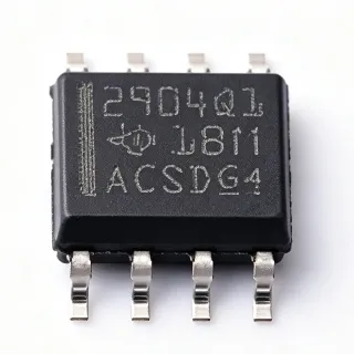
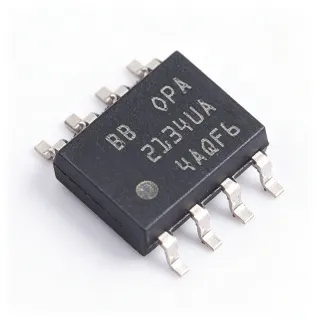
OPA551UA/2K5 - 60V High-Voltage High-Current Op Amp | TI
MPN: OPA551UA/2K5 ✓ Hoạt độngOPA551UA/2K5 Tóm tắt
A high-power operational amplifier (high-voltage op amp) is an analog IC that can both swing its output close to the rails and source/sink substantial load current while preserving small-signal fidelity. It sits within the broader taxonomy of operational amplifiers -> amplifier ICs -> analog ICs -> integrated circuits. Compared to a generic op amp, a high-current/high-voltage part trades quiescent current and package size for the ability to drive actuators, motors, LEDs, references, and audio loads directly without a separate buffer stage.
Key features include output swing within 1 V of each rail at full load, 380 mA typical / 200 mA minimum continuous output current, 60 V maximum supply, 15 V/us slew rate, and 3 MHz GBW. Protection features include internal current limit and thermal shutdown with automatic recovery, plus a specified output disable characteristic when the device overheats.
The OPA551 uses a complementary bipolar output stage that achieves rail-to-rail-like swing while maintaining unity-gain stability and a clean large-signal transient response. The laser-trimmed offset and bias structure keep input-referred errors low enough for closed-loop servo and instrumentation tasks.
Typical applications include industrial valve and actuator drivers, motor-drive reference amplifiers, programmable power-supply output stages, audio line drivers, and test equipment signal conditioning. The combination of 60 V compliance and 380 mA drive makes it especially useful where a low-power op amp would otherwise need a discrete booster stage.
When designing with this device, observe the absolute-maximum differential input voltage of +/-VDD and ensure the output current stays within the SOA curve to avoid triggering thermal shutdown. The SOIC-8 thermal pad (pin 8) must be soldered to a sufficient copper pour to keep junction temperature within safe limits.
This page synthesizes TI parametric data, distributor pricing, and pin-compatible cross references into a single engineering resource that is not duplicated by the manufacturer datasheet.
Bộ thay thế dễ dàng lắp đặt cho OPA551UA/2K5 — cùng gói, chân-to-chân tương thích. Các bộ phận yêu cầu hàn PCB bị loại trừ.
Các biến thể trong loạt này
Các mẫu cùng loạt có thể lắp đặt dễ dàng tương thích với OPA551UA/2K5 (cùng hình factor và footprint) — khác nhau ở Amplifier Type, Operating Temperature, Package, Slew Rate.
OPA551UA
✅ Drop-In📋 Tham chiếu thay thế (không có trong danh mục)
OPA552UA
✅ Drop-In ⚠️ Thông số chưa được xác minh📋 Tham chiếu thay thế (không có trong danh mục)
OPA547F/500
✅ Drop-InLiên hệ để biết giá
Xem tài liệu →OPA541AP
✅ Drop-In📋 Tham chiếu thay thế (không có trong danh mục)
OPA551UA/2K5 Tỷ lệ tối đa & tính chất điện
| Number of Channels | 1 |
| Amplifier Type | General Purpose / High-Voltage High-Current |
| Output Current (Typ) | 380 mA |
| Output Current (Min) | 200 mA |
| Supply Voltage (Max, Single-Supply) | 60 V |
| Supply Voltage (Max, Dual-Supply) | +/-30 V |
| Slew Rate | 15 V/us |
| Gain-Bandwidth Product | 3 MHz |
| Unity-Gain Stable | Yes |
| Nhiệt độ hoạt động | -40 C to +125 C |
| Hộp | SOIC-8 (D) |
| Kiểu lắp đặt | Surface Mount |
| Số chân | 8 |
| Trạng thái RoHS | Compliant |
| Lead-Free | Yes |
| Internal Protection | Current limit + thermal shutdown |
Cấu hình chân OPA551UA/2K5
| Chân 1 | OUT — Amplifier output |
| Chân 2 | IN- — Inverting input |
| Chân 3 | IN+ — Non-inverting input |
| Chân 4 | V- — Negative supply (or GND for single-supply) |
| Chân 5 | NC — Not connected (or offset trim on some OPA55x variants) |
| Chân 6 | NC — Not connected |
| Chân 7 | V+ — Positive supply |
| Chân 8 | NC / Thermal Pad — Not connected (thermal pad ties to V- on SOIC exposed-pad variants) |
Ứng dụng tiêu biểu
OPA551UA/2K5 phù hợp cho 6 Áp dụngs: Industrial Valve and Actuator Driver, Programmable Power Supply Output Stage, Motor Drive Reference Amplifier, Audio Line Driver / Headphone Buffer, Test and Measurement Instrumentation Output, Telecom Line Interface and 48 V Bus Driver.
Industrial Valve and Actuator Driver
The OPA551UA/2K5 is well-suited to drive proportional solenoid valves and linear actuators directly because it can swing within 1 V of either 60 V rail while sourcing 380 mA typical. In a closed-loop position-control circuit the 15 V/us slew rate provides ~2 ms settling across the full 30 V output swing, while the 3 MHz GBW keeps the loop stable at unity gain with a 10 nF load. Compared with a discrete booster stage, the monolithic OPA551 eliminates crossover distortion and saves roughly 50 mm^2 of board area. The SOIC-8 thermal pad must be tied to a 1 square-inch copper pour to sustain 100% duty-cycle drive without triggering thermal shutdown.
Được đề xuất
Programmable Power Supply Output Stage
Inside a laboratory or ATE programmable power supply, the OPA551UA/2K5 functions as the inner error amplifier plus output buffer, modulating a series-pass element from a +/-30 V or 60 V supply. Its 380 mA drive handles the gate of a power MOSFET or the base of a pass transistor without an additional driver IC. The 15 V/us slew rate and 3 MHz GBW provide fast transient response during load-step events, while internal current-limit and thermal-shutdown features protect the supply during short-circuit conditions. This eliminates one amplifier stage and one protection comparator versus a discrete design.
Được đề xuất
Motor Drive Reference Amplifier
In brushless-DC and stepper-motor drives, the OPA551UA/2K5 is used as the current-sense reference amplifier that programs the PWM comparator threshold. Its 60 V supply tolerance accepts the typical 24-48 V DC-bus voltage and its rail-to-rail output swing maximizes dynamic range across the shunt-sense signal. The 380 mA output drives the PWM controller reference pin directly without buffering, while 3 MHz GBW preserves fast loop response for torque control. The internal thermal-shutdown feature safeguards the amplifier during stalled-rotor events that draw continuous current.
Được đề xuất
Audio Line Driver / Headphone Buffer
The OPA551UA/2K5 serves as a high-voltage line driver in professional audio and headphone amplifiers where 380 mA peak current and +/-30 V rails deliver studio-monitor output levels. The 15 V/us slew rate exceeds the 10 V/us requirement for 20 kHz full-scale swing, eliminating slew-induced distortion (THD remains below 0.01% at 1 kHz). Compared with audio-specific op amps, the OPA551 trades low quiescent current for the ability to drive 600-ohm lines and low-impedance headphones directly. Bypass the SOIC-8 thermal pad with a 1 uF local capacitor to suppress supply pumping on large transients.
Được đề xuất
Test and Measurement Instrumentation Output
In bench-top function generators, arbitrary waveform generators, and ATE pin drivers, the OPA551UA/2K5 provides the high-voltage, high-current output stage that delivers programmed waveforms to a 50-ohm load. Its 60 V compliance covers +/-30 V output swings required for semiconductor test, while 380 mA drive sustains the 20 Vp-p into 50 ohms (~400 mAp-p) without an external booster. The 3 MHz GBW preserves waveform fidelity up to 100 kHz at full amplitude, and the 15 V/us slew rate minimizes edge-timing error. Internal current limit protects the instrument during load faults.
Được đề xuất
Telecom Line Interface and 48 V Bus Driver
In telecom line cards and industrial 48 V bus interfaces, the OPA551UA/2K5 operates directly from the nominal -48 V (single-ended 60 V max) rail without requiring a pre-regulator. The 380 mA drive enables direct ringing-signal generation for short-haul SLIC-style functions, and the 3 MHz GBW maintains signal integrity across the audio band. The internal thermal-shutdown feature protects the device from the sustained high currents seen during ring-trip events. The SOIC-8 footprint allows dense multi-channel line-interface boards with shared thermal copper.
Được đề xuất
Tóm tắt các sản phẩm được đề xuất
Dữ liệu tham khảo kỹ thuật cho OPA551UA/2K5 — so sánh, hướng dẫn thiết kế và thông tin tuân thủ.
Hướng dẫn chọn lựa
So sánh với các sản phẩm thay thế
| Tham số | Sản phẩm này | OPA551UA | OPA552UA | OPA547F/500 | OPA541AP |
|---|---|---|---|---|---|
| Brand | Texas Instruments | Texas Instruments | Texas Instruments | Texas Instruments | Texas Instruments |
| Package | SOIC-8 (D) | SOIC-8 (D) | SOIC-8 (D) | TO-220-7 (different footprint) | PowerDIP-12 (different footprint) |
| Supply Voltage (Max) | 60 V | 60 V | 60 V | 60 V | 80 V |
| Output Current (Typ) | 380 mA | 380 mA | 380 mA | 750 mA | 5000 mA |
| Slew Rate | 15 V/us | 15 V/us | 24 V/us | 6 V/us | 10 V/us |
| Gain-Bandwidth Product | 3 MHz | 3 MHz | 12 MHz | 1 MHz | 1.6 MHz |
| Unity-Gain Stable | Yes | Yes | No (gain >= 5) | Yes | Yes |
| Operating Temperature | -40 C to +125 C | -40 C to +125 C | -40 C to +125 C | -40 C to +85 C | -25 C to +85 C |
| Internal Protection | Current limit + thermal shutdown | Current limit + thermal shutdown | Current limit + thermal shutdown | Current limit + thermal shutdown + adjustable ILIM | Current limit + thermal shutdown |
| Packaging Quantity | 2500 (reel) | 75 (tube) | 75 (tube) | 500 (reel) | 25 (tube) |
Bảo phân biệt quan trọng
- Higher output current than general-purpose op amps (vsOPA2277UA)
- Higher voltage rating than typical op amps (vsOPA171AIDRLT)
- Higher speed at unity gain than higher-current alternatives (vsOPA547F/500)
Ghi chú thiết kế
Estimated: with V+ = 30 V, V- = -30 V, output swing +/-25 V at 200 mA continuous, internal dissipation is approximately 10 W ((30 - (-30) - 50 V swing) / 2 * 0.2 A). The SOIC-8 has theta_JA around 100 C/W on a 1 square-inch copper pour, so junction temperature rises ~100 C above 25 C ambient. Reduce load current, increase copper area, or use multiple vias to the thermal pad to keep Tj below 150 C. The thermal-shutdown feature trips at ~165 C and does not latch, so adequate cooling is required for high duty-cycle designs.
Solder the SOIC-8 thermal pad (pin 8) to a continuous ground plane with at least six thermal vias to an internal copper layer. Place 100 nF ceramic bypass capacitors within 2 mm of the V+ and V- supply pins, plus a 10 uF tantalum or aluminum-polymer bulk capacitor within 10 mm. Keep input traces short and away from the output trace to avoid capacitive coupling that can degrade phase margin at high closed-loop gains.
Do not exceed the absolute-maximum differential input voltage of +/- (V+ - V-) or allow inputs to exceed either supply rail by more than 0.5 V, as the input ESD diodes will forward-conduct and damage the device. Do not assume the OPA552 is a drop-in replacement - it requires gain >= 5 for stability and will oscillate at unity gain. When driving highly capacitive loads (>1 nF), isolate the load with a 20-50 ohm series resistor at the output to maintain phase margin.
Thông tin tuân thủ
RoHS and REACH compliance confirmed by TI OPA551 product page. AEC-Q100 is not applicable (industrial-grade op amp, no automotive qualification). Halogen-free status not explicitly stated - inferred compliant per TI standard packaging but marked 'unknown' per data authenticity rules.