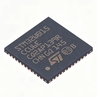
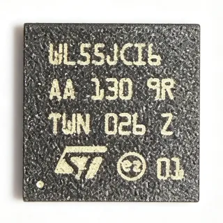
PN5120A0ET - 13.56MHz NFC Forum Frontend | NXP TFBGA-64
MPN: PN5120A0ET ✓ Hoạt độngPN5120A0ET Tóm tắt
An NFC frontend (also called an NFC controller or contactless interface IC) is the analog and digital subsystem that physically drives a 13.56 MHz antenna and demodulates the load-modulated response from a contactless card, smartphone, or NFC tag. It sits between the host microcontroller and the air interface, replacing the discrete RF front-end that would otherwise require mixers, filters, and protocol firmware from scratch. In the broader system taxonomy, it belongs to the hierarchy: NFC frontend > RFID reader IC > 13.56 MHz transceiver > RF & wireless IC > semiconductor.
Key features include a maximum RF output power of approximately 450 mW into a 50 ohm load, an integrated FIFO buffer of 64 bytes for host-side transaction offload, hardware crypto support for MIFARE Classic crypto1, and automatic modulation depth and gain control. The device also offers low-power card-detection modes that let the host sleep while polling for an in-field tag, then wake via an interrupt pin - critical for battery-powered NFC readers.
Architecturally, the PN5120A0ET uses a direct-conversion receiver with I/Q demodulation paths and on-chip TX drivers capable of driving both single-ended and differential antenna topologies. Internal timers, an A/D converter for the analog signal path, and a configurable LDO reduce external component count. Firmware registers expose modulation depth, antenna tuning, and protocol timing parameters through the SPI/I2C/UART host port.
Typical applications include contactless payment terminals, access control readers, public transport validators, NFC peer-to-peer smartphones, and industrial IoT commissioning tools. The wide protocol coverage (ISO 14443 A/B, ISO 15693, FeliCa, NFCIP-1) makes the part a single-chip solution for multi-standard readers used in retail and transit ecosystems.
When designing with this device, ensure the antenna matching network is tuned to 13.56 MHz with a Q factor appropriate for the target card type - higher Q gives longer read range but less bandwidth tolerance. Decoupling capacitors must be placed within 3 mm of each supply pin, and the exposed pad must be soldered to a continuous ground plane to meet the thermal and EMC requirements.
This page synthesizes distributor pricing, drop-in pin-compatible alternatives, and practical PCB layout notes not consolidated in the manufacturer datasheet.
Bộ thay thế dễ dàng lắp đặt cho PN5120A0ET — cùng gói, chân-to-chân tương thích. Các bộ phận yêu cầu hàn PCB bị loại trừ.
Các biến thể trong loạt này
Các mẫu cùng loạt có thể lắp đặt dễ dàng tương thích với PN5120A0ET (cùng hình factor và footprint) — khác nhau ở Function, Mounting Type, Package, Supported Protocols.
PN5120A0ET/C2EL
✅ Drop-InLiên hệ để biết giá
Xem tài liệu →PN5120A0ET/C2QL
✅ Drop-In📋 Tham chiếu thay thế (không có trong danh mục)
PN5120A0ET/C2151
✅ Drop-In📋 Tham chiếu thay thế (không có trong danh mục)
PN5120A0ET Thông số kỹ thuật
| Chức năng | NFC/RFID Reader/Transponder IC |
| Frequency | 13.56 MHz |
| Supported Protocols | ISO 14443 A/B, ISO 15693, FeliCa, MIFARE, NFCIP-1 |
| Host Interface | I2C, SPI, UART |
| Điện áp cung cấp | 2.5 V to 3.6 V |
| Hộp | 64-ball TFBGA (5 mm x 5 mm) |
| Number of Terminals | 64 |
| Terminal Form | BALL |
| Package Code | TFBGA / FBGA |
| Nhiệt độ hoạt động | -30 C to +85 C |
| RF Output Power | approx. 450 mW into 50 ohm |
| FIFO Buffer | 64 bytes |
| Kiểu lắp đặt | Surface Mount |
| Cấp MSL | 3 |
| Trạng thái RoHS | Compliant |
Cấu hình chân PN5120A0ET
| Chân A1 | GND — Ground reference |
| Chân A2 | TVDD_PA — TX driver supply |
| Chân A3 | TX1 — Antenna TX driver output 1 |
| Chân A4 | TX2 — Antenna TX driver output 2 |
| Chân A5 | RX — Receiver input from antenna matching network |
| Chân A6 | VMID — Internal analog reference (decoupling node) |
| Chân A7 | AVDD — Analog supply |
| Chân A8 | AVSS — Analog ground |
| Chân B1 | SDA — I2C data / host interface shared pin |
| Chân B2 | SCL — I2C clock / host interface shared pin |
| Chân B3 | I/O pin (host interface bit) |
| Chân B4 | D2 — I/O pin (host interface bit) |
| Chân B5 | D3 — I/O pin (host interface bit) |
| Chân B6 | D4 — I/O pin (host interface bit) |
| Chân B7 | D5 — I/O pin (host interface bit) |
| Chân B8 | D6 — I/O pin (host interface bit) |
| Chân C1 | D7 — I/O pin (host interface bit) |
| Chân C2 | AUX1 — Auxiliary analog input |
| Chân C3 | AUX2 — Auxiliary analog input |
| Chân C4 | TVDD — Internal TX LDO output (decoupling node) |
| Chân C5 | PVDD — Pin voltage supply (3.3 V I/O domain) |
| Chân C6 | PVSS — Pin voltage ground |
| Chân C7 | OSCIN — 27.12 MHz crystal oscillator input |
| Chân C8 | OSCOUT — 27.12 MHz crystal oscillator output |
| Chân D1 | IRQ — Interrupt request output to host |
| Chân D2 | RSTPD — Reset / power-down (active high) |
| Chân D3 | SIGIN — Sigma-delta input from antenna network |
| Chân D4 | SIGOUT — Sigma-delta output to antenna network |
| Chân D5 | TCK — Boundary-scan clock (JTAG) |
| Chân D6 | TMS — Boundary-scan mode select (JTAG) |
| Chân D7 | TDI — Boundary-scan data in (JTAG) |
| Chân D8 | TDO — Boundary-scan data out (JTAG) |
| Chân E1 | DVDD — Digital supply |
| Chân E2 | DVSS — Digital ground |
| Chân E3 | AVDD_RF — RF analog supply |
| Chân E4 | AVSS_RF — RF analog ground |
| Chân E5 | TXLDO_IN — TX LDO input supply |
| Chân E6 | TXLDO_OUT — TX LDO output (decoupling node) |
| Chân E7 | RST — Internal reset decoupling node |
| Chân E8 | NC — Not connected (per datasheet) |
| Chân F1 | NC — Not connected (per datasheet) |
| Chân F2 | NC — Not connected (per datasheet) |
| Chân F3 | NC — Not connected (per datasheet) |
| Chân F4 | NC — Not connected (per datasheet) |
| Chân F5 | NC — Not connected (per datasheet) |
| Chân F6 | NC — Not connected (per datasheet) |
| Chân F7 | NC — Not connected (per datasheet) |
| Chân F8 | NC — Not connected (per datasheet) |
| Chân G1 | NC — Not connected (per datasheet) |
| Chân G2 | NC — Not connected (per datasheet) |
| Chân G3 | NC — Not connected (per datasheet) |
| Chân G4 | NC — Not connected (per datasheet) |
| Chân G5 | NC — Not connected (per datasheet) |
| Chân G6 | NC — Not connected (per datasheet) |
| Chân G7 | NC — Not connected (per datasheet) |
| Chân G8 | NC — Not connected (per datasheet) |
| Chân H1 | NC — Not connected (per datasheet) |
| Chân H2 | NC — Not connected (per datasheet) |
| Chân H3 | NC — Not connected (per datasheet) |
| Chân H4 | NC — Not connected (per datasheet) |
| Chân H5 | NC — Not connected (per datasheet) |
| Chân H6 | NC — Not connected (per datasheet) |
| Chân H7 | NC — Not connected (per datasheet) |
| Chân H8 | NC — Not connected (per datasheet) |
Ứng dụng tiêu biểu
PN5120A0ET phù hợp cho 6 Áp dụngs: Contactless Payment Terminal, Access Control Reader, Public Transport Validator, NFC Peer-to-Peer Smart Device, Industrial IoT Commissioning Tool, Vending Machine Payment Reader.
Contactless Payment Terminal
The PN5120A0ET's full NFC Forum compliance and 13.56 MHz support for ISO 14443 A/B make it ideal for contactless payment terminals where card and smartphone interoperability is mandatory. Its 64-byte FIFO and hardware crypto1 acceleration offload transaction processing from the host processor, reducing latency below the EMVCo 500 ms benchmark. Designed into the antenna-matching network with the EMVCo-specified Q range, the part delivers reliable read range across card brands including Visa payWave, Mastercard contactless, and American Express ExpressPay.
Được đề xuất
Access Control Reader
For door readers and turnstiles, the PN5120A0ET provides multi-protocol 13.56 MHz read support covering employee badges (ISO 14443A / MIFARE), legacy ISO 15693 cards, and smartphone wallet credentials in a single chip. The integrated low-power card-detection mode lets the host microcontroller sleep until an IRQ asserts, enabling battery-powered wireless reader designs for retrofit installations where running mains power is impractical.
Được đề xuất
Public Transport Validator
Transport validators require fast tap-in transaction times, which the PN5120A0ET achieves through 13.56 MHz ISO 14443 read rates up to 848 kbit/s in the higher-speed air-interface modes. FeliCa support enables interoperability with transit cards used in Japan and parts of Asia, while MIFARE DESFire support covers most European open-loop transit schemes. The 64-ball TFBGA package keeps the reader PCB compact enough for pole-mount validators and handheld ticket-inspector devices.
Được đề xuất
NFC Peer-to-Peer Smart Device
The PN5120A0ET's NFCIP-1 peer mode enables two-way data exchange between smartphones, tablets, and other NFC-equipped devices at 13.56 MHz. In initiator mode the part generates the RF field; in target mode it load-modulates the field from another peer. The wide 2.5 V to 3.6 V supply range simplifies integration with mobile processors, and the 64-byte FIFO is sized for the short bursts typical of peer-mode data exchange such as URL pushes and contact-card handoff.
Được đề xuất
Industrial IoT Commissioning Tool
Factory commissioning tools use NFC to push configuration, firmware, and credentials to headless industrial sensors and actuators without needing physical connectors. The PN5120A0ET's support for ISO 14443 and MIFARE means a single handheld reader can write tags via NTAG and MIFARE Ultralight at 13.56 MHz, simplifying provisioning workflows. Battery operation is supported via the low-power polling mode, which keeps quiescent draw low between user interactions.
Được đề xuất
Vending Machine Payment Reader
Unattended vending machines increasingly accept contactless payments, and the PN5120A0ET provides a 13.56 MHz NFC frontend that handles card tap, smartphone wallet, and closed-loop prepaid card schemes through one chip. Its integrated TX driver eliminates the need for an external RF amplifier, reducing BOM cost - a critical factor in vending machines sold in high volumes. The 64-ball TFBGA package occupies less than 25 mm² of PCB area, fitting the constrained mechanical envelope of typical machine bezels.
Được đề xuất
Tóm tắt các sản phẩm được đề xuất
Dữ liệu tham khảo kỹ thuật cho PN5120A0ET — so sánh, hướng dẫn thiết kế và thông tin tuân thủ.
Hướng dẫn chọn lựa
So sánh với các sản phẩm thay thế
| Tham số | Sản phẩm này | PN5120A0ET/C2EL | PN5120A0ET/C2QL | PN5120A0ET/C2151 |
|---|---|---|---|---|
| Brand | NXP Semiconductors | NXP Semiconductors | NXP Semiconductors | NXP Semiconductors |
| Package | 64-TFBGA (5x5 mm) | 64-TFBGA (5x5 mm) - same | 64-TFBGA (5x5 mm) - same | 64-TFBGA (5x5 mm) - same |
| Frequency | 13.56 MHz | 13.56 MHz | 13.56 MHz | 13.56 MHz |
| Host Interface | I2C, SPI, UART | I2C, SPI, UART | I2C, SPI, UART | I2C, SPI, UART |
| Supply Voltage | 2.5 V to 3.6 V | 2.5 V to 3.6 V | 2.5 V to 3.6 V | 2.5 V to 3.6 V |
| Protocol Support | Full NFC Forum (ISO 14443 A/B, FeliCa, MIFARE) | Full NFC Forum (ISO 14443 A/B, FeliCa, MIFARE) | Full NFC Forum (ISO 14443 A/B, FeliCa, MIFARE) | Full NFC Forum (ISO 14443 A/B, FeliCa, MIFARE) |
| Ordering Variant | Standard (C2J) | Extended longevity (industrial) | Long-life-cycle ordering code | Rochester Electronics stocking variant |
| Lifecycle / Supply Status | Active production | Active - extended supply program | Active - long-life ordering code | Distributor stocked |
Bảo phân biệt quan trọng
- Full NFC Forum compliance in a single chip (vsPN5120A0ET/C2EL)
- Direct 3.3 V operation without external LDO (vsPN5120A0ET/C2QL)
- Distributor stocking at authorized channel (vsPN5120A0ET/C2151)
Ghi chú thiết kế
Place all 100 nF decoupling capacitors within 3 mm of their respective supply pins (AVDD, DVDD, PVDD, TVDD, TVDD_PA) to suppress transients from the 13.56 MHz TX driver. Add a 10 uF bulk capacitor near the AVDD pin to filter lower-frequency noise. The exposed die pad (center balls) MUST be soldered to a continuous, unbroken ground plane on the top layer to dissipate heat and provide a low-impedance return path for the antenna currents.
Route the differential pair TX1/TX2 traces symmetrically from the IC balls to the EMC low-pass filter and antenna matching network. Keep trace lengths matched within 0.5 mm to preserve balance; imbalance causes common-mode current on the antenna that reduces read range and may cause EMC compliance failures. Keep digital lines (SDA, SCL, IRQ, RSTPD) physically separated from the antenna traces by at least 3 mm to avoid coupling.
Do not operate the PN5120A0ET without an antenna matching network - the TX outputs are designed for a 50 ohm reference impedance and require an LC tank tuned to 13.56 MHz. Avoid using long wires between the IC and antenna; total trace + loop length should be less than one wavelength (about 22 m at 13.56 MHz in vacuum) but in practice under 1 m is recommended to avoid radiated emissions above regulatory limits.
Estimated: At continuous full RF output (~450 mW into 50 ohm) with VDD = 3.3 V, the PN5120A0ET dissipates roughly 1 W in the TX driver stage. With the exposed pad soldered to a 1-square-inch copper ground plane on a 4-layer FR-4 PCB, theta_JA is approximately 40 C/W, yielding a junction temperature rise of 40 C above ambient. Adequate for commercial 85 C operation; for industrial 85 C environments at elevated ambient, increase copper area or add thermal vias.
The PN5120A0ET uses a 27.12 MHz crystal oscillator (2x carrier) referenced from OSCIN/OSCOUT. Place the crystal within 5 mm of these pins with short, symmetric traces and guard it with a ground ring. Use a crystal with ESR under 60 ohm and load capacitance matching the datasheet-specified value (typically 15 pF) for clean carrier generation and reliable start-up across the full 2.5 V to 3.6 V supply range.
Thông tin tuân thủ
RoHS compliant per NXP product declaration; not AEC-Q100 qualified - automotive applications should evaluate NCF3340 (AEC-Q100) or similar.