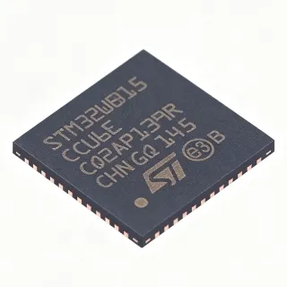
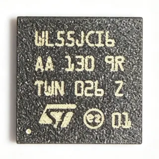
PN7160A1EV-C100K - NFC Controller, 13.56MHz, NCI, VFBGA-64 | NXP
MPN: PN7160A1EV-C100K ✓ Hoạt độngPN7160A1EV-C100K Tóm tắt
An NFC controller is a dedicated mixed-signal IC that handles the 13.56 MHz RF front-end (including modulation, demodulation, antenna tuning, and EMV/NFC framing) so that the host application processor does not need to manage real-time RF timing. Within the broader hierarchy, the PN7160A1EV sits as an NFC controller -> contactless reader/writer -> RF front-end IC -> wireless connectivity semiconductor. By offloading the entire ISO stack and providing integrated firmware (with NCI 2.0 host commands), the part enables fast integration into Android, Linux, RTOS, and bare-metal hosts without RF design expertise.
Key features include up to 1.5 W RF output power, integrated EMVCo 3.1 and NFC Forum certification-ready firmware, automatic antenna tuning via an external variable capacitor bridge, integrated temperature monitoring, and low-power card-detection polling. The VFBGA-64 (4 mm x 4 mm) package supports compact PCB layouts typical of smartphones, tablets, payment terminals, and IoT devices. The host communicates over standard I2C up to 3.4 MHz, simplifying integration with most application processors.
Architecturally, the PN7160A1EV uses a dedicated ARM Cortex-M0 microcontroller core running the integrated NFC firmware, an RF analog front-end supporting all major modulation schemes (ASK 10%/100%, BPSK), a power management unit with multiple LDO regulators, and an integrated balun-less transmitter requiring only an EMC filter. The device automatically manages RF collision avoidance, CRC, and anti-collision, reducing host MCU load. The /C100K suffix indicates firmware revision and packaging variant; the /C100 firmware is the latest production release, while the trailing K denotes a specific reel or production line code.
Typical applications include NFC contactless payment terminals, smartphone and tablet NFC modems, smart wearables with payment/ticketing, IoT devices with tap-to-pair or NFC commissioning, and access-control readers. The combination of high RF output and integrated EMVCo-compliant firmware is especially valuable for payment-grade terminals where certification time is critical.
When designing with this part, antenna matching is the single most important step: use the NXP NFC Cockpit configuration tool to tune the matching network and TXLDO voltage to the specific antenna geometry. The two VDD rails (1.8 V host I/O and 3.3 V RF/transmitter) must be decoupled with 100 nF + 1 µF ceramic capacitors placed within 2 mm of the supply balls. Always reserve GPIO/DWL_REQ for the host-to-controller interrupt handshake, and follow the reference PCB layout in the datasheet (controlled-impedance differential feed to the antenna pads, solid RF ground plane under the IC).
This page synthesizes distributor pricing, drop-in alternatives, and practical design notes not found in the manufacturer datasheet alone, providing engineers with a single-source reference for NFC controller selection.
Bộ thay thế dễ dàng lắp đặt cho PN7160A1EV-C100K — cùng gói, chân-to-chân tương thích. Các bộ phận yêu cầu hàn PCB bị loại trừ.
Các biến thể trong loạt này
Các mẫu cùng loạt có thể lắp đặt dễ dàng tương thích với PN7160A1EV-C100K (cùng hình factor và footprint) — khác nhau ở Package, Function, Host Interface, MSL Level, Mounting Type.
PN7160A1EV-C100Y
✅ Drop-InLiên hệ để biết giá
Xem tài liệu →PN7161A1EV-C100K
✅ Drop-InLiên hệ để biết giá
Xem tài liệu →PN7161A1EV-C100Y
✅ Drop-InLiên hệ để biết giá
Xem tài liệu →PN7160A1EV-C100K Thông số kỹ thuật
| Chức năng | NFC Controller with NCI Interface |
| Operating Frequency | 13.56 MHz |
| Supported Standards | ISO 14443 (A/B), ISO 15693, FeliCa, MIFARE, NFC Forum R/W, P2P, CE |
| Host Interface | I2C up to 3.4 MHz; NCI 2.0 |
| Supply Voltage VDD (Host I/O) | 1.65 V to 1.95 V |
| Supply Voltage VBAT/PVDD | 3.0 V to 3.6 V |
| RF Output Power | Up to 1.5 W |
| Hộp | 64-VFBGA (4 mm x 4 mm) |
| Khoảng nhiệt độ hoạt động | -40 C to +85 C |
| Firmware | Integrated NCI-compliant firmware (NXP) |
| Card Emulation | Type A/B, FeliCa, ISO 15693 |
| Antenna Tuning | Automatic via external variable capacitor bridge |
| Host OS Support | Android, Linux, RTOS, bare-metal |
| Trạng thái RoHS | Compliant |
| Kiểu lắp đặt | Surface Mount (BGA) |
| Cấp MSL | 3 |
Cấu hình chân PN7160A1EV-C100K
| Chân A1 | GND — Ground |
| Chân A2 | VBAT — Battery/PA supply 3.0-3.6 V |
| Chân A3 | PVDD — RF transmitter supply |
| Chân A4 | TX1 — RF output driver 1 |
| Chân A5 | TX2 — RF output driver 2 |
| Chân A6 | VANT — Antenna tuning supply |
| Chân A7 | ANT1 — Antenna tuning DAC 1 |
| Chân A8 | ANT2 — Antenna tuning DAC 2 |
| Chân B1 | GND — Ground |
| Chân B2 | VDD — Host I/O supply 1.65-1.95 V |
| Chân B3 | RST — Reset (active low) |
| Chân B4 | IRQ — Host interrupt request |
| Chân B5 | SDA — I2C data |
| Chân B6 | SCL — I2C clock |
| Chân B7 | GPIO0 — General purpose I/O 0 |
| Chân B8 | GPIO1 — General purpose I/O 1 |
| Chân C1 | GND — Ground |
| Chân C2 | RF1P — RF input positive (from antenna) |
| Chân C3 | RF1N — RF input negative (from antenna) |
| Chân C4 | RF2P — Differential RF signal positive |
| Chân C5 | RF2N — Differential RF signal negative |
| Chân C6 | GPIO2 — General purpose I/O 2 |
| Chân C7 | GPIO3 — General purpose I/O 3 |
| Chân C8 | DWL_REQ — Firmware download request |
| Chân D1 | GND — Ground |
| Chân D2 | RXN — Receiver input negative |
| Chân D3 | RXP — Receiver input positive |
| Chân D4 | AUX_RF — Auxiliary RF signal |
| Chân D5 | VCC_TXLDO — Transmitter LDO output |
| Chân D6 | TEST — Test mode (must be grounded in normal operation) |
| Chân D7 | NC — Not connected |
| Chân D8 | NC — Not connected |
Ứng dụng tiêu biểu
PN7160A1EV-C100K phù hợp cho 6 Áp dụngs: NFC Contactless Payment Terminals, Smartphone and Tablet NFC Modems, Smart Wearables with Tap-to-Pay / Ticketing, IoT Devices with NFC Commissioning / Tap-to-Pair, Access Control and Door Readers, Industrial / Consumer Electronics with NFC Diagnostics.
NFC Contactless Payment Terminals
The PN7160A1EV-C100K's integrated EMVCo 3.1 firmware, up to 1.5 W RF output, and automatic antenna tuning make it ideal for payment terminals requiring PCI-PTS and EMVCo L1 certification. Placed between the antenna loop and the application processor, it handles all 13.56 MHz RF modulation, anti-collision, and ISO 14443 A/B framing for Visa payWave, Mastercard contactless, and similar schemes. Unlike a discrete RF front-end + host stack, the integrated NCI 2.0 firmware cuts certification cycle time from months to weeks, since EMVCo loopback and digital protocol tests are pre-validated.
Được đề xuất
Smartphone and Tablet NFC Modems
The PN7160A1EV-C100K is widely adopted in Android smartphones for NFC modem operation across reader/writer, peer-to-peer, and card-emulation modes. With a 1.8 V host I/O rail matching application processors and a low-power polling mode for battery operation, it integrates cleanly into mobile PMIC rails. The 4 mm x 4 mm VFBGA-64 footprint suits space-constrained handset designs. Compared with solutions requiring host-side ISO stack, it offloads real-time RF work to the internal Cortex-M0 core, leaving the application processor free for application tasks.
Được đề xuất
Smart Wearables with Tap-to-Pay / Ticketing
Wearables with NFC payment or transit-ticketing require compact, low-power 13.56 MHz interfaces. The PN7160A1EV-C100K's 4 mm x 4 mm VFBGA, 1.8 V host interface, and low-power card-detection polling (~uA range when properly duty-cycled) suit smartwatch and fitness-band designs. The integrated firmware supports card-emulation Type A/B and FeliCa for global transit ticketing. The automatic antenna-tuning path accommodates small-loop wearable antennas where Q-factor and detuning vary with the wearer's body proximity.
Được đề xuất
IoT Devices with NFC Commissioning / Tap-to-Pair
IoT products increasingly use NFC for out-of-band commissioning (Wi-Fi/BLE credential transfer, secure provisioning). The PN7160A1EV-C100K provides the peer-to-peer and reader/writer modes needed to read NFC tags (NTAG, ST25) and exchange NDEF messages with smartphones. Its NCI 2.0 host interface works with Linux and RTOS, and the integrated firmware means the IoT MCU only needs to forward NCI commands without implementing ISO stack. The 3.3 V RF rail draws well under 100 mA during active RF transmission, suitable for battery-powered commissioning flows.
Được đề xuất
Access Control and Door Readers
Access-control readers using MIFARE Classic, MIFARE DESFire, ISO 14443, and ISO 15693 credentials benefit from the PN7160A1EV-C100K's broad protocol coverage and high RF output. With 1.5 W RF power, the read range extends to the typical 5-10 cm required for door-mounted readers. The integrated NCI firmware handles anti-collision for multiple cards presented simultaneously and supports secure element extensions via host commands, allowing credential migration to mobile credentials without hardware changes.
Được đề xuất
Industrial / Consumer Electronics with NFC Diagnostics
Industrial printers, smart appliances, and consumer electronics embed NFC for diagnostics, firmware update, or parameter setting via smartphone tap. The PN7160A1EV-C100K supports tag-reading (NTAG, MIFARE Ultralight) and NDEF message exchange with minimal host overhead. The 3.0-3.6 V RF supply and -40 to +85 C operating range suit industrial environments. Compared with simple tag-reader-only ICs, the PN7160A1EV's full NFC Forum compliance future-proofs the design for P2P or card-emulation modes if added later.
Được đề xuất
Tóm tắt các sản phẩm được đề xuất
Dữ liệu tham khảo kỹ thuật cho PN7160A1EV-C100K — so sánh, hướng dẫn thiết kế và thông tin tuân thủ.
Hướng dẫn chọn lựa
So sánh với các sản phẩm thay thế
| Tham số | Sản phẩm này | PN7160A1EV-C100Y | PN7161A1EV-C100K | PN7161A1EV-C100Y |
|---|---|---|---|---|
| Package | VFBGA-64 (4x4 mm) | VFBGA-64 (4x4 mm) - same | VFBGA-64 (4x4 mm) - same | VFBGA-64 (4x4 mm) - same |
| Brand | NXP Semiconductors | NXP Semiconductors | NXP Semiconductors | NXP Semiconductors |
| Operating Frequency | 13.56 MHz | 13.56 MHz | 13.56 MHz | 13.56 MHz |
| Host Interface | I2C + NCI 2.0 | I2C + NCI 2.0 | I2C + NCI 2.0 | I2C + NCI 2.0 |
| Supply Voltage VDD | 1.65-1.95 V | 1.65-1.95 V | 1.65-1.95 V | 1.65-1.95 V |
| Supply Voltage VBAT | 3.0-3.6 V | 3.0-3.6 V | 3.0-3.6 V | 3.0-3.6 V |
| Apple ECP Support | No | No | Yes (after authorization) | Yes (after authorization) |
| RF Output Power | Up to 1.5 W | Up to 1.5 W | Up to 1.5 W | Up to 1.5 W |
Bảo phân biệt quan trọng
- Integrated NCI 2.0 firmware stack with EMVCo 3.1 and NFC Forum certification (vsST25R3916 (STMicroelectronics RF front-end))
- Up to 1.5 W RF output with automatic antenna tuning (vsPN7150 (previous-generation NXP NFC controller))
- Pin-compatible upgrade path to Apple ECP via PN7161 (vsPN7161A1EV-C100K (NXP variant with ECP))
Ghi chú thiết kế
Place the 64-VFBGA on a dedicated ground plane with all GND balls stitched to the plane via short vias to minimize parasitic inductance on the 13.56 MHz RF path. The differential RF trace from RF1P/RF1N to the EMC filter and antenna matching network should be 50 ohm controlled-impedance, kept as short as possible, with no signal vias. Maintain a continuous solid ground pour under and around the IC and the antenna feed. A 4-layer PCB with dedicated ground plane (layer 2) and power plane (layer 3) is recommended for EMVCo compliance.
Decouple both VDD (1.8 V) and VBAT/PVDD (3.3 V) rails with a 100 nF X7R ceramic capacitor within 2 mm of each supply ball, plus a bulk 1 µF to 4.7 µF ceramic. The TXLDO output (VCC_TXLDO) requires its own 10 µF bulk capacitor to support peak RF transmit current. Sequencing: bring up VBAT first or simultaneously with VDD; do not apply VDD without VBAT present, as the internal LDOs may not initialize correctly. A power-on-reset circuit or simple RC delay on RST is recommended for slow-rising supplies.
Do not connect the TEST ball to anything other than ground in production; floating TEST may put the device in test mode and prevent normal operation. The DWL_REQ pin is intended only for firmware download; do not use it as a regular GPIO. Always run the NXP NFC Cockpit configuration tool to tune the antenna matching network and TXLDO voltage for the specific antenna PCB geometry, antenna Q-factor, and target card location - a non-tuned antenna can reduce read range by 30-50% and fail EMVCo certification.
Estimated: at continuous RF transmission (1.5 W RF output) and 3.3 V VBAT, the PN7160A1EV-C100K can draw up to ~250 mA from VBAT, dissipating roughly 0.5-0.8 W internally in the TX path and LDOs. The 4 mm x 4 mm VFBGA-64 has a theta_JA of approximately 35-45 C/W (depending on PCB copper area). For continuous RF operation above ambient, ensure the GND balls are stitched to a continuous 2 cm x 2 cm copper pour on top and bottom layers. Duty-cycled transmission (typical for NFC poll-list) avoids sustained thermal stress.
Thông tin tuân thủ
RoHS compliant per NXP product page and DigiKey listing. AEC-Q100 not applicable - this is a consumer/mobile NFC controller, not an automotive-grade part. Halogen-free status not explicitly stated in available data.