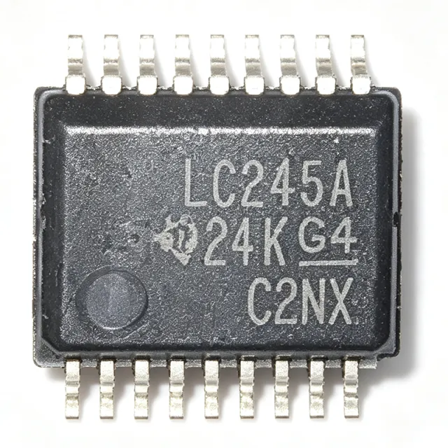
SN74LVC240A - Octal Inverting Buffer 3-State LVC | TI
MPN: SN74LVC240A ✓ Hoạt độngSN74LVC240A Tóm tắt
An octal buffer/line driver is a digital logic IC in the 74xx logic family that provides signal buffering, inversion, and bus isolation. Within the logic-IC hierarchy, the SN74LVC240A belongs to the Low-Voltage CMOS (LVC) technology family, a subfamily of 74-series logic. Its 3-state outputs allow multiple devices to share a common bus without contention, a fundamental requirement in bus-oriented digital systems such as memory subsystems and backplanes.
Key features include 5.5-V tolerant inputs enabling mixed-mode signal operation on all ports (5-V input/output voltage support), a typical propagation delay (tpd) of 3.3 ns at VCC = 3.3 V, and low typical VOLP (output ground bounce) and VOHV (output VOH undershoot) figures for superior signal integrity. According to the TI datasheet (SCAS293), the device can drive a load with total capacitance less than or equal to 50 pF while still meeting all datasheet specifications.
The device is built on advanced CMOS technology, combining low static power consumption with high noise immunity and strong output drive. The dual-bank structure with separate active-low output-enable (OE) inputs supports half-duplex transceiver topologies and word-wide bus gating. When OE is low, data passes from the A inputs to the inverted Y outputs; when OE is high, outputs enter the high-impedance state.
Typical applications include 3-state memory address and clock driving, 3.3-V to 5-V mixed-voltage bus interfacing, industrial control I/O buffering, and telecom line-card logic. Packages include SOIC-20 (DW), TSSOP-20 (PW), and SSOP-20 (DB).
Design tip: keep total capacitive load at or below 50 pF for guaranteed timing, add 0.1 uF decoupling per supply pin, and tie unused inputs to VCC or GND to prevent floating-node oscillation.
Bộ thay thế dễ dàng lắp đặt cho SN74LVC240A — cùng gói, chân-to-chân tương thích. Các bộ phận yêu cầu hàn PCB bị loại trừ.
Các biến thể trong loạt này
Các mẫu cùng loạt có thể lắp đặt dễ dàng tương thích với SN74LVC240A (cùng hình factor và footprint) — khác nhau ở Output Type.
SN74LV240A
Liên hệ để biết giá
Xem tài liệu →SN74LVC240A-Q1
📋 Tham chiếu thay thế (không có trong danh mục)
SN74AHCT240A
📋 Tham chiếu thay thế (không có trong danh mục)
74LVC240APW
📋 Tham chiếu thay thế (không có trong danh mục)
74LVC240AMTC
📋 Tham chiếu thay thế (không có trong danh mục)
74LVC240APW-13
📋 Tham chiếu thay thế (không có trong danh mục)
SN74LVC240A Tỷ lệ tối đa & tính chất điện
| Chức năng | Octal inverting buffer/driver with 3-state outputs |
| Supply Voltage Range | 1.65 V to 3.6 V |
| Nominal Operating Voltage | 3.3 V |
| Input Tolerance | 5.5 V regardless of VCC |
| Kênh | 8 (two 4-bit banks with separate OE) |
| Kiểu đầu ra | 3-state, inverting |
| Propagation Delay (tpd) | 3.3 ns typ at VCC = 3.3 V |
| Max Capacitive Load | 50 pF (for guaranteed datasheet specs) |
| Packages | SOIC-20 (DW), TSSOP-20 (PW), SSOP-20 (DB) |
| Kiểu lắp đặt | Surface Mount |
| Logic Family | LVC (Low-Voltage CMOS) |
| Output Enable | Active-low OE per 4-bit bank |
| Trạng thái RoHS | Compliant |
Cấu hình chân SN74LVC240A
| Chân 1 | 1OE — Output enable, bank 1 (active low) |
| Chân 2 | 1A1 — Bank 1 input 1 |
| Chân 3 | 2Y4 — Bank 2 output 4 (inverted, 3-state) |
| Chân 4 | 2A4 — Bank 2 input 4 |
| Chân 5 | 2Y3 — Bank 2 output 3 (inverted, 3-state) |
| Chân 6 | 2A3 — Bank 2 input 3 |
| Chân 7 | 2Y2 — Bank 2 output 2 (inverted, 3-state) |
| Chân 8 | 2A2 — Bank 2 input 2 |
| Chân 9 | 2Y1 — Bank 2 output 1 (inverted, 3-state) |
| Chân 10 | GND — Ground |
| Chân 11 | 2A1 — Bank 2 input 1 |
| Chân 12 | 1Y1 — Bank 1 output 1 (inverted, 3-state) |
| Chân 13 | 1A2 — Bank 1 input 2 |
| Chân 14 | 1Y2 — Bank 1 output 2 (inverted, 3-state) |
| Chân 15 | 1A3 — Bank 1 input 3 |
| Chân 16 | 1Y3 — Bank 1 output 3 (inverted, 3-state) |
| Chân 17 | 1A4 — Bank 1 input 4 |
| Chân 18 | 1Y4 — Bank 1 output 4 (inverted, 3-state) |
| Chân 19 | 2OE — Output enable, bank 2 (active low) |
| Chân 20 | VCC — Power supply, 1.65 V to 3.6 V |
Ứng dụng tiêu biểu
SN74LVC240A phù hợp cho 6 Áp dụngs: Memory Address and Clock Driving, 3.3V to 5V Mixed-Voltage Bus Interfacing, Industrial Control I/O Buffering, Bus-Oriented Receivers and Transmitters, Telecom Line-Card Logic, Microcontroller Peripherals and GPIO Expansion.
Memory Address and Clock Driving
The SN74LVC240A is purpose-built per the TI datasheet (SCAS293) to improve the performance and density of 3-state memory address drivers and clock drivers. Its 3.3-ns typical propagation delay and 50-pF guaranteed capacitive drive keep address and clock edges sharp across DRAM/SRAM buses, while 3-state outputs let the processor, DMA, and test logic share address lines without contention. Two independently enabled 4-bit banks allow half-bus gating during refresh or boot modes. Place parts close to the memory connector and keep stubs under the 50-pF load budget for guaranteed timing.
Được đề xuất
3.3V to 5V Mixed-Voltage Bus Interfacing
Thanks to 5.5-V tolerant inputs independent of VCC, the SN74LVC240A accepts legacy 5-V logic signals while running from a 3.3-V rail, per TI datasheet SCAS293. This supports mixed-mode signal operation on all ports - a 3.3-V-powered board can directly receive 5-V microcontroller or backplane outputs without clamp diodes or series protection. Outputs swing to 3.3 V, so use it on paths where the receiving 5-V device recognizes 3.3-V levels (true for most TTL-threshold inputs). This eliminates level-shifting ICs on receive-only paths, saving BOM cost and board area.
Được đề xuất
Industrial Control I/O Buffering
In PLC I/O racks and industrial control boards, the SN74LVC240A buffers sensor and actuator logic signals with strong CMOS drive and high noise immunity across a 1.65-V to 3.6-V supply. The dual-bank, independently enabled 3-state structure isolates I/O groups during configuration or fault conditions, and the low VOLP ground-bounce specification keeps switching transients off shared ground planes in electrically noisy factory environments. Its wide -40C-to-125C-grade availability and low per-channel cost (about $0.03/channel at volume) make it economical for high channel-count buffering.
Được đề xuất
Bus-Oriented Receivers and Transmitters
The SN74LVC240A fits backplane and board-level bus transceiver architectures where the TI datasheet (SCAS293) explicitly targets bus-oriented receivers and transmitters. 3-state outputs allow multiple line cards or peripherals to drive a shared data bus under OE control, and the inverting function pairs with non-inverting buffers (such as the LVC244) to build latch-through or XOR-parity bus topologies. Low typical VOHV output undershoot protects neighboring receiver inputs during simultaneous switching, supporting reliable multi-drop communication at 3.3-V logic speeds.
Được đề xuất
Telecom Line-Card Logic
Telecom line cards use the SN74LVC240A for address decoding buffers, clock distribution to SLIC/SLAC devices, and 3-state isolation of shared control buses during hot-swap or maintenance windows. The 5.5-V tolerant inputs accept legacy 5-V control signals common in carrier equipment, while the device runs on the modern 3.3-V card rail. Its low static CMOS power consumption reduces per-card dissipation across high-density shelves, and SOIC-20/TSSOP-20 packages suit both wave-soldered and reflow line-card assembly processes used in telecom manufacturing.
Được đề xuất
Microcontroller Peripherals and GPIO Expansion
Around MCUs such as the MSP430 and TMS320 families, the SN74LVC240A expands buffered GPIO, drives LED/status arrays through current-limiting resistors, and isolates shared peripheral buses (memory-mapped displays, FPGAs, external SRAM) during reset. The separate 1OE/2OE enables let firmware gate I/O banks independently, and 3-state outputs prevent bus fight between the MCU and FPGA during configuration. Its 3.3-ns delay adds negligible timing overhead to MCU bus cycles, and the 5-V tolerant inputs safely interface 5-V legacy modules.
Được đề xuất
Tóm tắt các sản phẩm được đề xuất
Dữ liệu tham khảo kỹ thuật cho SN74LVC240A — so sánh, hướng dẫn thiết kế và thông tin tuân thủ.
Hướng dẫn chọn lựa
So sánh với các sản phẩm thay thế
| Tham số | Sản phẩm này | SN74LV240A | SN74LVC240A-Q1 | 74LVC240APW | SN74AHCT240A |
|---|---|---|---|---|---|
| Package | TSSOP-20 (PW) | TSSOP-20 (PW) - same | TSSOP-20 (PW) - same | TSSOP-20 (PW) - same | TSSOP-20 (PW) - same |
| Brand | Texas Instruments | Texas Instruments | Texas Instruments | Nexperia | Texas Instruments |
| 5.5V-Tolerant Inputs | Yes | No | Yes | Yes | N/A (5V supply) |
| Function | Inverting, 3-state, dual 4-bit banks | Inverting, 3-state - same | Inverting, 3-state - same | Inverting, 3-state - same | Inverting, 3-state - same |
| Automotive Grade | No | No | Yes (AEC-Q100) | No | No |
| Best For | Mixed 3.3V/5V bus interfacing | Cost-driven 3.3V buffering | Automotive designs | Second-source supply | 5V CMOS logic domains |
Bảo phân biệt quan trọng
- 5.5-V tolerant inputs on a 3.3-V rail (vsSN74LV240A)
- Automotive qualification available (vsSN74LVC240A-Q1)
- Wide low-voltage supply range (vsSN74AHCT240A)
Ghi chú thiết kế
Per TI datasheet SCAS293, the SN74LVC240A guarantees all specifications only when total capacitive load is at or below 50 pF. In high-speed bus designs, budget trace capacitance (roughly 1-2 pF per cm of PCB trace) plus receiver input capacitance against this 50-pF limit. For heavier loads, series-terminate (22-33 ohm) to control edge rate and reflections, or split the bus across more drivers.
Place a 0.1 uF ceramic decoupling capacitor within 2-3 mm of each VCC pin, with one bulk 4.7-10 uF capacitor per group of octal buffers. Simultaneous switching of eight outputs can induce ground bounce; the datasheet's low typical VOLP specification is achieved only with a solid, low-inductance ground return - use vias directly to the ground plane at pin 10.
Tie unused inputs to VCC or GND - never leave them floating, as floating CMOS inputs can oscillate and increase static current. Remember the outputs are inverting: a LOW input produces a HIGH output. OE pins are active-low, so pull OE high (or use a pullup) during power-up if bus contention must be avoided until firmware takes control.
Thông tin tuân thủ
Standard TI catalog logic device, RoHS compliant; confirm exact suffix (-NOPB) material declarations on TI product page. AEC-Q100 version available as SN74LVC240A-Q1.




