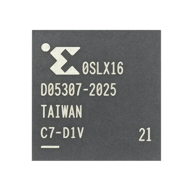
XC6SLX16-2CPG196I - 14k Logic Cells Spartan-6 FPGA | AMD
MPN: XC6SLX16-2CPG196I ✓ Hoạt động| Số lượng | Giá đơn vị | Phụ |
|---|---|---|
| 1 | $163.125 | $163,13 |
| 10 | $117.8125 | $1.178,13 |
| 100 | $104.2187 | $10.421,87 |
| 500 | $99.6875 | $49.843,75 |
| 1.000 | $95.1563 | $95.156,30 |
XC6SLX16-2CPG196I Tóm tắt
A Field Programmable Gate Array (FPGA) is a semiconductor integrated circuit built from configurable logic blocks (CLBs), programmable routing, and dedicated hardware resources such as block RAM, multipliers/DSP slices, and clock management tiles (DCMs/PLLs). The Spartan-6 LX series sits in the low-power, low-cost tier of the AMD/Xilinx product hierarchy: FPGA -> programmable logic -> logic IC -> integrated circuit. Spartan-6 LX devices target high-volume, cost-sensitive bridging, control, and signal-processing applications that need the parallelism and reconfigurability of an FPGA without the cost of a Virtex-class device.
Key features of the XC6SLX16-2CPG196I include: 14,579 logic cells (~2,300 logic slices), 106 maximum user I/Os (some version/board use this number; package allows up to 106), 576 Kbit (72 Kbyte) of block RAM, 32 DSP48A1 slices, four DCMs and two PLLs for clock management, on-chip memory controllers (MCB) for DDR/DDR2/LPDDR, and a 1.2 V core supply with dedicated high-performance/low-power transceiverless I/O banks. The device is implemented on 45 nm process technology, delivering low static and dynamic power versus previous Spartan generations. The -2 speed grade is the mid-tier in the Spartan-6 family and balances Fmax and power for typical industrial designs.
Architecturally, the XC6SLX16-2CPG196I uses a register-rich, columnar LUT-6 architecture with dedicated carry chains, distributed RAM/SRL16 shift-register logic in each CLB, and a hard PCIe endpoint block on higher-density siblings (note: LX16 does not include the integrated PCIe block; it is on LX45+). Multiple I/O standards (LVCMOS, LVDS, HSTL, SSTL) are supported with per-bank reference voltages, and the package is lead-free (Pb-free) RoHS-compliant. The 8 × 8 mm CSBGA package supports high-density board layouts in space-constrained designs.
Typical applications include industrial motor control and factory automation, automotive infotainment displays and driver-assistance modules, consumer video bridging (HDMI/LVDS), low-cost software-defined radio front-ends, embedded vision pre-processing, and communication backplane bridging. The 576 Kbit of block RAM and 32 DSP slices make the LX16 well suited to small FIR/IIR filters, modest FFT engines, sensor-fusion pre-processing, and glue-logic aggregation. Pairing with a small external SPI flash for configuration memory keeps the BOM lean.
When designing with this FPGA, verify that the -2 speed grade meets your target Fmax for the design floorplan, ensure JTAG and DONE pull-up values match the Spartan-6 configuration user guide, and check I/O-bank voltage compatibility before mixing 3.3 V peripherals with 1.2 V core logic. Note: the LX16 does not include the integrated PCIe block; use LX45/LX75/LX100/LX150 if PCIe hard IP is required.
This page synthesizes AMD/Xilinx datasheet specifications, distributor pricing as of 2026-10-11, same-package drop-in alternatives within the Spartan-6 family, and practical design notes.
Bộ thay thế dễ dàng lắp đặt cho XC6SLX16-2CPG196I — cùng gói, chân-to-chân tương thích. Các bộ phận yêu cầu hàn PCB bị loại trừ.
Các biến thể trong loạt này
Các mẫu cùng loạt có thể lắp đặt dễ dàng tương thích với XC6SLX16-2CPG196I (cùng hình factor và footprint) — khác nhau ở Operating Temperature, Package, Process Technology, Speed Grade, Block RAM.
Công cụ so sánh nhanh — Chọn các bộ phận thay thế để so sánh song song:
XC6SLX16-3CPG196C
Liên hệ để biết giá
Xem tài liệu →XC6SLX16-2CPG196C
Liên hệ để biết giá
Xem tài liệu →XC6SLX25-2CPG196C
📋 Tham chiếu thay thế (không có trong danh mục)
XC6SLX45-2CPG196C
📋 Tham chiếu thay thế (không có trong danh mục)
XC6SLX9-2CPG196C
📋 Tham chiếu thay thế (không có trong danh mục)
XC6SLX16-2CPG196I Tỷ lệ tối đa & tính chất điện
| Product Series | Spartan-6 LX |
| Part Number | XC6SLX16-2CPG196I |
| Manufacturer | AMD (formerly Xilinx) |
| Logic Cells | 14,579 |
| Slices | 2,278 (each = 4 LUTs + 8 FFs) |
| Block RAM | 576 Kbit (72 Kbyte) |
| DSP Slices | 32 (DSP48A1) |
| Maximum User I/Os | 106 |
| Core Voltage | 1.2 V nominal |
| Speed Grade | -2 |
| Nhiệt độ hoạt động | -40 °C to +100 °C (industrial, "I" suffix) |
| Hộp | 196-ball CSBGA / TFBGA, 8 mm × 8 mm |
| Package Code | CPG196 |
| Process Technology | 45 nm CMOS, 9-metal copper, low-k |
| Clock Management | 4 DCMs + 2 PLLs |
| Memory Controller Blocks | 2 MCBs (DDR/DDR2/LPDDR) |
| Configuration Memory Interface | SPI, BPI, JTAG, Master Serial |
| RoHS Compliance | RoHS-compliant (lead-free) |
Cấu hình chân XC6SLX16-2CPG196I
| Chân A1 | GND — Ground (per AMD Spartan-6 CPG196 ballmap) |
| Chân A2 | IO_L1N_0 — Bank 0 I/O, lower-left leg of LVDS pair (L1_N) |
| Chân A3 | IO_L2N_0 — Bank 0 I/O, lower-left leg of LVDS pair (L2_N) |
| Chân B1 | VCCINT_1 — Core 1.2 V supply (sector 1) |
| Chân C8 | CCLK — Configuration clock input (master mode) / output (slave mode) |
| Chân D9 | DONE — Configuration completion flag, open-drain; 4.7 kΩ pull-up recommended |
| Chân E10 | TCK — JTAG test clock input |
| Chân F11 | TDI — JTAG test data in |
| Chân G12 | TDO — JTAG test data out |
| Chân H13 | TMS — JTAG test mode select |
| Chân K5 | VCCAUX_2 — 2.5 V auxiliary supply (sector 2) |
| Chân L6 | VCCO_3 — Bank 3 I/O supply (1.2 - 3.3 V) |
| Chân M7 | GND_LVDS — LVDS reference ground for bank-pair |
| Chân N8 | PROG_B — Program/reset input, active low |
| Chân P9 | INIT_B — Configuration init (active low open-drain) |
| Chân B11 | M0 — Configuration mode pin M0 (sets master/slave SPI/JTAG mode) |
| Chân C12 | M1 — Configuration mode pin M1 |
| Chân E13 | HSWAPEN — Hot-swap enable for I/O during configuration |
| Chân K13 | NC — Not connected (per package ballmap) |
| Chân L13 | NC — Not connected (per package ballmap) |
Ứng dụng tiêu biểu
XC6SLX16-2CPG196I phù hợp cho 7 Áp dụngs: Industrial Motor Control and Factory Automation, Automotive Infotainment and HMI Bridging, Low-Cost Software-Defined Radio Front-End, Embedded Vision and Image Pre-Processing, Communication Bridge and Protocol Aggregator, IoT Edge Sensor Aggregation and AI Pre-Processor, Test and Measurement Instrumentation.
Industrial Motor Control and Factory Automation
The XC6SLX16-2CPG196I is a strong fit for industrial motor control and factory automation because its 32 DSP48A1 slices provide the 18×18 multiply-accumulate throughput needed for vector-control (FOC) loops at 10–50 kHz, while the 576 Kbit of block RAM holds reference-angle lookup tables, observed PI-state histories, and modest PID overshoot buffers without needing an external SRAM. Industrial -40°C to +100°C operation is guaranteed by the I temperature suffix, supporting outdoor or cabinet-edge mounting. The 106 user I/Os ease connection to multi-axis incremental encoders (QEP inputs), PWM pairs (6 axes ×2 = 12 lines), and 24 V opto-isolated digital I/O through HSTL/LVCMOS banks. Compared with a fixed-function motor-control MCU, the LX16 also allows on-chip HMI/Modbus-TCP gateware and a MicroBlaze soft CPU without external glue logic. Built-in memory controller blocks can attach a DDR2 chip for multi-axis parameter storage, eliminating a parallel footprint. Practical example: a 4-axis FOC drive fits comfortably in ~30 percent of LX16 LUTs and 24 DSP48A1 slices, with margin to add safety state machines and a panel-HMI interface. For an industrial-grade PCB, the 8×8 mm CSBGA manages routing for high-PWM-edge-rate tracks while keeping heat dissipation in spec (Tj ≤ +100 °C).
Được đề xuất
Automotive Infotainment and HMI Bridging
The XC6SLX16-2CPG196I is well suited to low-end automotive infotainment and human-machine interface bridging because its 14,579 logic cells and 106 user I/Os provide the resource budget to bridge LVDS or OpenLDI display panels with HDMI/MIPI-CSI sources while sustaining modest video overlays. The industrial-grade temperature range covers vehicle cabin ambient, while the 576 Kbit block RAM supports frame-buffers for 800×480 displays at 16 bpp partial-update regions. The two memory controller blocks allow external DDR2 to capture framebuffers, removing the need for parallel SRAM. Compared with a fixed-function bridge ASIC, the LX16 lets a Tier-1 car maker add a new codec or in-cabin gesture feature by bitstream update, reducing tooling cost. The 32 DSP slices handle color-space conversion (RGB↔YUV) and light gamma correction without bottlenecks. Spartan-6 LX tier cost targets aggressive automotive display-bridge price points at sub-$25 BOM. Should a higher-bandwidth (e.g. 1080p) display pipeline arise, migration to LX45-CPG196 (same footprint) is footprint-compatible, providing a graceful Fmax- and RAM-upgrade pathway.
Được đề xuất
Low-Cost Software-Defined Radio Front-End
The XC6SLX16-2CPG196I is an effective FPGA for low-cost software-defined radio and signal-intelligence front-ends because its 32 DSP48A1 slices are dense enough to implement 64-tap digital-channelization FIR filters and a 256-point radix-2 FFT for narrow-band FM/AM/voice at IF sample rates up to ~40 MSPS, while the 576 Kbit of block RAM captures 4-ms-length capture windows at 8-bit IQ samples without external memory. The four DCMs and two PLLs are usable to generate independent sample-rate and reference-clock domains from a single 10–50 MHz reference. Spartan-6 LX tier offers low static and dynamic power at 1.2 V, allowing a battery-operated SDR dongle. Industrial temperature grade supports outdoor C2X or ham-radio field-deployment. The 106 user I/Os accept parallel ADC/DAC buses such as 14-bit ×8 lanes for direct ADC decimation. Compared with a discrete DSP, the LX16 allows the user to swap demod algorithms via SPI bitstream update, enabling post-sale SDR feature releases without retooling. Practical example: a multi-band receiver from 70 MHz to 6 GHz (with mixer/RF frontend) fits in ~60 percent of LX16 logic and 25 DSP slices, leaving margin for a soft CPU and a USB-UART bridge.
Được đề xuất
Embedded Vision and Image Pre-Processing
The XC6SLX16-2CPG196I is practical for embedded-vision front-ends because its 32 DSP48A1 slices can compute Bayer-to-RGB color conversion, 3×3 Sobel edge detection, and small-window histogram equalization at 30 fps at resolutions up to 1.3 megapixel (1280×1024), and the 576 Kbit of block RAM holds at least one full line-buffer at 16-bit precision (approx. 1280 pixels × 16-bit × 4 lines = ~10 Kbit per line, easily fit). The 14,579 logic cells also accept a small RISC-V (PicoRV32) soft-core for housekeeping and a Camera-Link or LVDS camera interface, all on the LX16 floorplan. The industrial -40°C to +100°C range allows outdoor robot cameras and machine-vision installations. The memory controller blocks support a DDR2 chip to capture full frames or to act as an extra line-buffer pool for Sobel, sharpening, and Laplacian filters. Compared with running vision on a Cortex-A-class SoC, the LX16 enables deterministic latency at low power, ideal for robotic-agriculture or roadside-camera sensors. Practical migration path: LX16 → LX25-CPG196 footprint-compatible when more tap-memory or larger line-buffers are needed.
Được đề xuất
Communication Bridge and Protocol Aggregator
The XC6SLX16-2CPG196I fits communication-bridge designs because its 106 user I/Os support mixed LVDS and LVCMOS peripherals in the same package, with HSTL and SSTL selectable per I/O bank. Bridge applications include UART/SPI/I2C ↔ GbE aggregation, SPI ↔ CAN-FD gateways, JTAG-over-USB bridges, and I2S ↔ TDM audio routers, all of which fit in roughly half the LX16 resources. The two PLLs and four DCMs handle clock-domain crossing between industrial 24 MHz crystal, reference clocks from upstream PHYs, and ASIX Ethernet. Industrial-grade support is required for cabinet and outdoor telecom installations. The 576 Kbit of block RAM can buffer Ethernet TX/RX frames up to several KB without needing external SRAM. Compared to a hard-bridge SoC, the LX16 enables fast-turnaround protocol customization (CC-Link, EtherCAT, etc.) by simply updating the bitstream. For higher-throughput 1Gbit/s packet-routing, the LX45 in the same CPG196 footprint offers faster DSP and 3x more logic.
Được đề xuất
IoT Edge Sensor Aggregation and AI Pre-Processor
The XC6SLX16-2CPG196I is widely used in IoT edge sensor aggregation hubs because its 14,579 logic cells can implement a small ML state machine (e.g. anomaly detection over accelerometer data), a few serial-protocol peripherals (I2C/SPI/UART), and a tiny soft MicroBlaze or PicoRV32 core, all in the 8×8 mm footprint. The 32 DSP slices can run 32-point cosine transforms or fixed-point FFTs at audio sampling rates for voice-keyword spotting, while the 576 Kbit block RAM captures sensor burst data. Industrial temperature ensures outdoor or factory-edge deployments. The memory controllers can attach LPDDR memory for sensor log spooling. Compared with an MCU-class aggregator, the LX16 enables simultaneous high-rate sensor burst sampling and decision logic in a deterministic fabric. Practical migration: the LX16 → LX25 → LX45 in CPG196 provides in-footprint scaling when more on-chip AI preprocessing is needed.
Được đề xuất
Test and Measurement Instrumentation
The XC6SLX16-2CPG196I is well matched to bench-instrument designs because its 106 user I/Os can drive parallel LED segment displays, rotary-encoder inputs, and analog-front-end triggers, while the 32 DSP slices perform 16-bit fixed-point spectrum analysis or adaptive-filter implementations in real time. The 14,579 logic cells accept a soft CPU (MicroBlaze or PicoRV32) for USB-CDC/HID command parsing and 4-wire SPI-to-FPGA configuration. The two PLLs cleanly derive the sample-rate clock from a precision 10 MHz OCXO or GPS-disciplined source. Industrial temperature is sufficient for bench-instrument chassis (typically 0–50 °C operating ambient). The 576 Kbit of block RAM supports loop-length capture buffers up to several KB. Compared to a fixed-function DSP, the LX16 also allows instrument firmware updates without opening the chassis. A test-and-measurement front-end typically uses ~70 percent of LX16 logic and leaves margin for FPGA Mezzanine Card (FMC) connectors, rear-panel sync, and option modules.
Được đề xuất
Tóm tắt các sản phẩm được đề xuất
Dữ liệu tham khảo kỹ thuật cho XC6SLX16-2CPG196I — so sánh, hướng dẫn thiết kế và thông tin tuân thủ.
Hướng dẫn chọn lựa
So sánh với các sản phẩm thay thế
| Tham số | Sản phẩm này | XC6SLX16-2CPG196C | XC6SLX16-3CPG196C | XC6SLX25-2CPG196C | XC6SLX45-2CPG196C | XC6SLX9-2CPG196C |
|---|---|---|---|---|---|---|
| Brand | AMD (Xilinx) | AMD (Xilinx) | AMD (Xilinx) | AMD (Xilinx) | AMD (Xilinx) | AMD (Xilinx) |
| Package | 196-ball CSBGA (CPG196) 8x8 mm | 196-ball CSBGA (CPG196) 8x8 mm - same | 196-ball CSBGA (CPG196) 8x8 mm - same | 196-ball CSBGA (CPG196) 8x8 mm - same | 196-ball CSBGA (CPG196) 8x8 mm - same | 196-ball CSBGA (CPG196) 8x8 mm - same |
| Logic Cells | 14,579 | 14,579 | 14,579 | 24,051 | 43,661 | 9,152 |
| Speed Grade | -2 | -2 | -3 (faster) | -2 | -2 | -2 |
| Temperature Grade | Industrial -40C to +100C | Commercial 0C to +85C | Commercial 0C to +85C | Commercial 0C to +85C | Commercial 0C to +85C | Commercial 0C to +85C |
| Block RAM | 576 Kbit | 576 Kbit | 576 Kbit | 936 Kbit | 2,088 Kbit | 270 Kbit |
| DSP Slices | 32 | 32 | 32 | 38 | 58 | 16 |
| Maximum User I/Os | 106 | 106 | 106 | 106 | 106 | 106 |
| PCIe Endpoint Hard IP | No | No | No | No | Yes (PCIe x1 endpoint) | No |
Bảo phân biệt quan trọng
- Footprint-compatible scaling across LX9 / LX16 / LX25 / LX45 / LX75 in CPG196 (vsXC6SLX9-2CPG196C)
- Industrial -40C to +100C operation vs commercial-grade LX16-2CPG196C (vsXC6SLX16-2CPG196C)
- Higher logic/RAM/DSP density than LX9, with same ballmap and supplier availability (vsXC6SLX16-3CPG196C)
Ghi chú thiết kế
The XC6SLX16-2CPG196I requires three rails: VCCINT at 1.2 V (±60 mV) for the core, VCCAUX at 2.5 V for clock/JTAG logic, and VCCO per-bank for I/O at 1.2-3.3 V standard. Decoupling follows the AMD/Xilinx Spartan-6 power management reference: one 33 uF and one 100 uF bulk cap per rail, plus 0.1 uF and 0.01 uF ceramics as close to each VCCINT/VCCAUX pin pair as possible. The DONE pin needs a 4.7 kΩ pull-up to 2.5 V; PROG_B and INIT_B also require pull-ups for proper configuration startup. All three rails must ramp within the Spartan-6 datasheet's required 25 ms window or the device may fail to configure; an MCU-supervisor or sequencer (e.g., TPS3808G50) is recommended for industrial power-rail sequencing.
The 8×8 mm CSBGA package has a theta-JA of roughly 30 °C/W with a moderate copper-area PCB. At industrial-grade operation (junction up to +100 °C), static power dominates before dynamic power at typical industrial clocking rates. For designs near the LX16 top utilization (>=70 percent LUT and 32 DSP running at 250 MHz), measure the board-thermal gradient in early prototypes; derate by 25 to 30 percent when planning for fan-less industrial chassis with +70 °C ambient. Spartan-6 LX uses 45 nm CMOS process, so leakage rises with junction temperature. Use XPower Analyzer inside ISE to estimate the static + dynamic worst-case. Avoid placing the LX16 next to >1 W switching regulators without at least 6 mm of isolation or a guard thermal fence.
Place the configuration SPI flash within 25 mm of the FPGA and keep the SPI traces matched-length within 1 mm to ensure reliable multi-I/O (x2/x4) configuration. Decoupling capacitors must be on the same layer with vias placed within 1 mm of the FPGA BGA land pattern. The 196-ball CSBGA with 0.5 mm pitch escapes on a 4-layer PCB require microvia-in-pad for efficient fanout; for 2-via escape, expect 12-15 mm of fanout per bank. Maintain constant trace-impedance of 50 Ω single-ended or 100 Ω differential for HSTL/SSTL DDR memory interfaces routed to the MCB blocks; route HSYNC-style clock-pair alongside data lanes to control skew. The DONE, PROG_B, and INIT_B traces should be kept short and pulled to 2.5 V VCCAUX to avoid false triggering during noisy system start.
Common pitfalls: (1) Using the wrong speed grade file for timing analysis - ISE timing closure done against -1 reduces Fmax headroom - always target the actual device speed grade (-2 in this case). (2) Forgetting the CCLK initial-state - master mode CCLK must be quiescent at startup; a noise-pumped CCLK causes bitstream load failures. (3) Crossing I/O banks with mixed HSTL/LVCMOS without setting VCCO per-bank correctly causes input-level violations and bus contention. (4) Setting JTAG M0/M1/TMS on the wrong mode pins means the device boots into a non-JTAG configuration mode (BPI/SPI master) and JTAG access fails. (5) The LX16 does not include PCIe hard IP - for PCIe x1 endpoint, choose LX45 or higher. (6) Verify completion of the bitstream CRC by monitoring DONE; spurious DONE-pull-during-config indicates a corrupt bitstream usually from SPI flash corruption or VCCINT ripple.
Thông tin tuân thủ
RoHS compliant per AMD/Xilinx product page, lead-free CPG196 ballmap is REACH and halogen-free; industrial temperature -40C to +100C; not AEC-Q100 qualified (for Grade-2 automotive AEC-Q100 equivalent, choose -3 industrial or XC6SLX16-2CSG324Q1Q-qualified variants in larger packages per AMD ordering guide).







