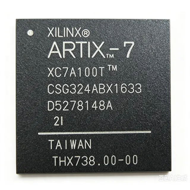
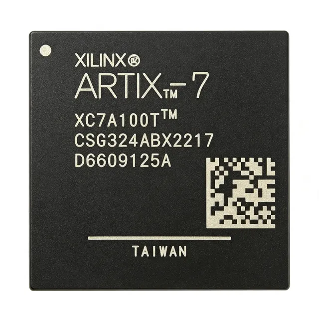
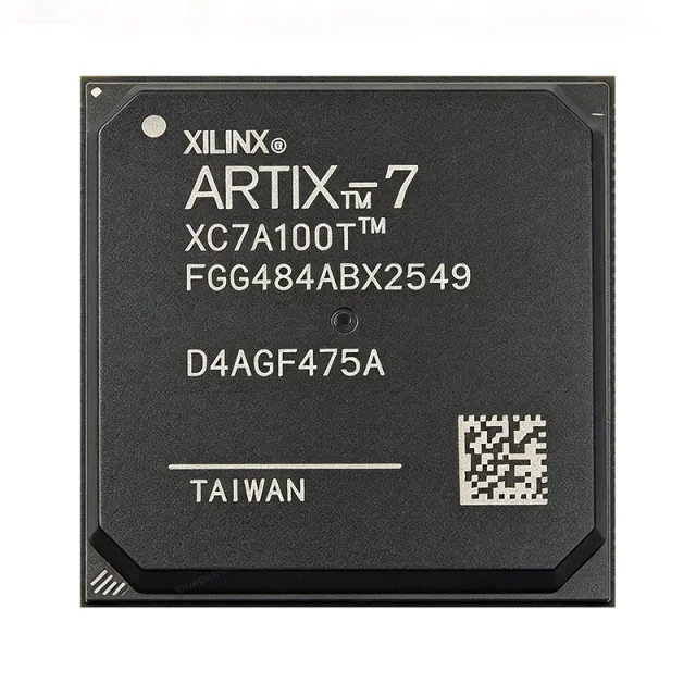
XC7A100T-2FGG484C
XC7A100T-2FGG484C - 101440-Cell Artix-7 FPGA | AMD
The AMD XC7A100T-2FGG484C is an Artix-7 field-programmable gate array with 101,440 FPGA logic cells, 285 I/O sites, and a 484-ball FCBGA package. It combines programmable logic, block RAM, DSP resources, mixed-signal blocks, MMCMs, and PLLs in a single device for cost-sensitive embedded, communications, instrumentation, and industrial control systems. The -2 speed grade and commercial-temperature suffix identify its device qualification position within the XC7A100T family.
An FPGA is a programmable digital semiconductor whose internal logic blocks, memory, and signal-processing resources are configured after manufacture. Within the product hierarchy, the XC7A100T belongs to the Artix-7 family, then to FPGA and CPLD devices, and ultimately to programmable logic semiconductors. Unlike a fixed-function application-specific integrated circuit, an FPGA can support multiple interface standards and logic functions while allowing design revisions without changing the PCB.
The device provides 101,440 logic cells and 285 I/O sites in the 484-FCBGA package. Search data also identifies MMCM and PLL clock-management resources. These resources support parallel data processing, timing generation, clock conditioning, interface bridging, control logic, and embedded signal-processing functions. The 484-ball package provides a high-density connection interface suitable for designs requiring numerous power, ground, configuration, clock, and user-I/O connections.
The XC7A100T implementation uses 28 nm FPGA technology, providing a balance between programmable logic density, performance, power consumption, and cost. Its architecture allows most I/O standards to be assigned in software through the FPGA development toolchain, although board-level voltage, signal-integrity, and power requirements still constrain the usable interface set. MMCM and PLL resources can multiply, divide, phase-shift, and condition clocks when a design needs deterministic timing relationships.
Typical uses include industrial automation, data-acquisition equipment, communications infrastructure, test and measurement systems, embedded control, and high-speed digital signal processing. A design can implement parallel buses, sensor interfaces, protocol converters, timing systems, and control algorithms in parallel, reducing the number of supporting discrete devices. The XC7A100T-2FGG484C is especially relevant to compact systems where 285 I/O sites and substantial programmable logic must fit a relatively dense package.
PCB design must follow the AMD package drawing, pinout files, and power-delivery recommendations exactly. Decoupling capacitors should be placed directly beside the associated power balls, configuration and programming signals require careful signal-integrity review, and unused package balls must follow the prescribed land-pattern and assembly guidance rather than being treated as ordinary no-connect pins.
This page combines the exact orderable MPN, package and resource details, compatible family options, practical PCB guidance, and structured comparisons to support design selection before schematic capture, footprint review, Vivado part assignment, and prototype release.
詢價
聯絡我們