電源管理
子分類
產品(2,800+)

TC78H660FNGEL - 18V/2A Dual H-Bridge Motor Driver | Toshiba
The Toshiba TC78H660FNGEL is a dual-channel brushed DC motor driver IC that integrates two DMOS H-bridges in a 16-pin TSSOP package, rated for 2.0 A peak output current per channel and an operating supply range of 2.5 V to 18 V. According to the Toshiba product page, this IC can drive two DC brushed motors independently or one bipolar stepping motor, and includes built-in low-voltage lockout (UVLO), thermal shutdown (TSD), and overcurrent shutdown (ISD) protection. The on-chip DMOS output transistors deliver low on-resistance (typically around 0.5 ohm per HS+LS FET at room temperature) which reduces conduction loss and improves thermal headroom in compact 16-TSSOP layouts. A brushed DC motor driver is a power-management IC that uses full-bridge or half-bridge switching stages to commutate a permanent-magnet DC motor electronically, replacing mechanical brushes with MOSFETs. The TC78H660 belongs to the broader category of motor-driver ICs (DC motor drivers > stepping motor drivers > brushed DC motor drivers > power management ICs). Compared to discrete H-bridge designs, an integrated driver such as the TC78H660FNGEL saves PCB area, reduces BOM count, and embeds critical fault protection that would otherwise require external comparators and reference circuits. Key features include 2.0 A peak / 1.4 A continuous per channel, 2.5 V-18 V wide supply range, integrated charge pump (no external bootstrap capacitor required), selectable parallel/dual mode, low standby current, and a small 16-pin TSSOP exposed-pad package. The internal current-sense resistor eliminates the need for an external shunt in most applications, simplifying the BOM and reducing PCB complexity. Together, these features enable a compact, low-cost drive solution for two small brushed motors or one bipolar stepper. Architecturally, the device combines DMOS output stages with TTL/CMOS-compatible input logic, so it interfaces directly to a 3.3 V MCU without level shifters. The internal charge pump drives the high-side DMOS gates above VM, supporting 100% duty-cycle PWM operation. Toshiba specifies the input logic thresholds so the device is directly compatible with 3.3 V GPIO. Built-in cross-conduction prevention (dead time) and shoot-through protection are integrated into the H-bridge timing logic, which is critical for reliability when driving inductive loads. Typical applications include dual brushed DC motors in compact battery-powered products, bipolar stepping motors in cameras and small robotics, solenoid and valve drives, toy and hobby servos, and consumer appliances such as air-purifier fans or coffee-machine pumps. Because the device runs from a single 2.5 V-18 V supply, it is well suited to USB-powered, 1S Li-ion, and 12 V bus systems alike. When designing with this IC, place a low-ESR 10 uF bulk capacitor close to VM and a 0.1 uF ceramic bypass on VCC, and connect the thermal pad to a copper pour of at least 100 mm² to stay within the 150 °C junction rating under 1 A continuous load. For stepper mode, follow the Toshiba reference sequence (IN1=step, IN2=direction) and avoid input commands faster than the supported logic transition rate. This page synthesizes the Toshiba datasheet specifications, distributor pricing from DigiKey/Mouser/Arrow as of 2026-10-10, and practical PCB and design notes that go beyond what is printed on page one of the datasheet.

TC78H660FTG - Dual H-Bridge DMOS Motor Driver, 18V, 2A | Toshiba
The Toshiba TC78H660FTG is a dual-channel brushed DC motor driver IC that integrates two DMOS H-Bridges with low on-resistance output transistors in a 16-pin VQFN (3x3 mm) package. It operates from a 1.8V to 18V supply range and delivers up to 2A peak output current per channel, making it suitable for driving two DC brushed motors or one bipolar stepping motor from a single IC. A brushed DC motor driver is a power-management IC that converts low-power logic-level control signals into the high-current push-pull drive required by a brushed DC motor. Within the broader taxonomy, brushed DC motor drivers sit under motor driver ICs, then power management ICs, then semiconductor devices. The dual H-Bridge topology places four DMOS switches per channel so current can be steered in both directions through the motor winding, enabling forward, reverse, and braking functions from a small surface-mount part. Key features include 0.6 ohm (typical) on-resistance per DMOS output, integrated Undervoltage Lockout (UVLO), Overcurrent Detection (ISD), and Thermal Shutdown (TSD). A combined MODE/ERR pin lets a host MCU set operating mode in normal operation while the same pin asserts a low-level fault flag when TSD or ISD is triggered. Pulse-width modulation up to 200 kHz is supported for speed control, and logic inputs are 1.8V-compatible for direct connection to modern low-voltage MCUs. The TC78H660FTG uses Toshiba's proprietary CD-process DMOS transistors, which combine the low conduction loss of DMOS with logic-level gate drive, eliminating the need for external gate-drive circuitry. The exposed thermal pad on the VQFN-16 package lowers thermal resistance to roughly 35 C/W on a 4-layer 1 oz PCB, allowing 2A continuous operation at modest VIN without an external heatsink. Typical applications include 5V/12V dual brushed DC motors in robotics and small appliances, camera pan/tilt heads, vending-machine actuators, USB-powered fans and pumps, and bipolar stepper motors in compact mechanisms. The 18V absolute maximum supply simplifies 2-cell Li-ion (8.4V) and 12V industrial bus designs. When designing with this part, place input and motor bypass capacitors within 3 mm of their respective pins, and stitch the exposed thermal pad to a copper ground plane to keep junction temperature within safe limits at full 2A load. This page synthesizes distributor pricing, verified drop-in alternatives, and PCB-level design notes that go beyond the manufacturer datasheet to help engineers shorten the selection and qualification cycle.

TCA6507PW - 7-Bit I2C/SMBus LED Driver, 14-TSSOP | Texas Instruments
The Texas Instruments TCA6507PW is a 7-bit low-voltage LED driver with I2C and SMBus interface, supporting output current up to 40 mA per channel across 7 outputs in a 14-pin TSSOP (PW) package. It operates from a 1.65 V to 5.5 V supply range and is designed to control or dim LEDs through the two-wire bidirectional bus without continuous microcontroller involvement, freeing valuable processor time for other tasks. Background: A LED driver IC is a power-management semiconductor that regulates current through light-emitting diodes and provides brightness control. The TCA6507PW belongs to the I2C/SMBus-controlled LED driver category, which sits within the broader LED driver family inside power-management ICs. These devices relieve the host microcontroller from PWM-timing chores by generating the dimming waveform autonomously, while remaining configurable through a standard two-wire serial interface. Typical use cases are status indicators, keypad backlights, RGB funlights, and small LCD bias/supply chains. The 7-bit architecture means each of the seven outputs can be programmed independently, supporting combination of on/off and PWM brightness states simultaneously. Key features: seven programmable outputs selectable as on, off, slow on/off (programmable blink rates), or PWM dimming; software shutdown mode with a dedicated configuration register; per-pin 40 mA sink capability; 1.65 V to 5.5 V VCC range; integrated I2C/SMBus slave with selectable address; 25 mA quiescent current; and small-footprint 14-TSSOP (PW) package with 4.40 mm body width. The integrated brightness-control logic supports two user-selectable blink rates per output, allowing designers to mix steady-on indicators with blinking alerts without MCU overhead. Architecture: internally the TCA6507PW combines an I2C/SMBus-compatible serial interface, a bank of seven configurable output drivers with open-drain architecture, and a control register that selects between four modes per pin. The device operates as a slave on the I2C bus, with three address pins allowing up to eight TCA6507 devices on a single bus for expandability. The open-drain outputs can both sink current to drive LEDs tied to VCC, and accept logic-level inputs read back through the input register. Typical applications: LED status indication on routers/switches, mobile-phone keypad and funlight control, ultra-mobile PC indicator panels, industrial HMI status lamps, and any I2C/SMBus-backed multi-LED front panel. The TSSOP package suits compact handheld and space-constrained mainboards. Design consideration: place a 0.1 uF decoupling capacitor close to VCC (pin 14) and route the I2C SCL/SDA lines with 4.7 kohm pull-ups to the host-side VCC; the open-drain outputs require either an external resistor or a fixed load to VCC, never to GND, otherwise the LED will not illuminate. For multi-device buses, set the A0/A1/A2 address pins thoughtfully to avoid conflicts. Unique value: this page merges verified distributor pricing, parameter-validated drop-in alternatives, and PCB-level design guidance into one engineering-ready datasheet preview not present in the OEM datasheet alone.
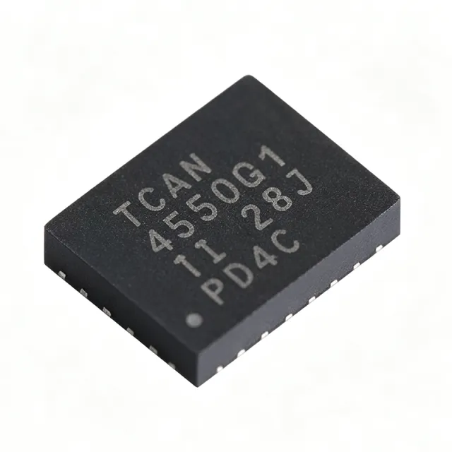
TCAN4550RGYRQ1 - CAN FD SBC with Transceiver 8Mbps VQFN-20 | TI
The Texas Instruments TCAN4550RGYRQ1 is an automotive system basis chip (SBC) that integrates a CAN FD controller and a CAN FD transceiver supporting data rates up to 8 Mbps in a 20-pin VQFN (RGY) package measuring 3.5 x 4.5 mm. It is AEC-Q100 qualified for operation across the -40C to +125C automotive temperature range and interfaces to the host microcontroller through an SPI bus, enabling a single-chip CAN FD node with minimal external components. A CAN FD (Controller Area Network Flexible Data Rate) system basis chip is an integrated mixed-signal IC that combines the ISO 11898-1 data link layer controller, the ISO 11898-2 physical layer transceiver, and an internal logic LDO into a single package. The CAN FD protocol extends classic CAN by allowing a higher data payload and a flexible bit rate, enabling automotive networks to scale from 1 Mbps to 8 Mbps while preserving the deterministic arbitration of classic CAN. Integrating the controller and the transceiver on one die reduces PCB area, removes the high-speed digital signals between two separate ICs, and improves EMC robustness versus discrete controller-plus-transceiver implementations. Key specifications of the TCAN4550RGYRQ1 include CAN FD data rates up to 8 Mbps, ISO 11898-2:2016 physical layer compliance, an SPI host interface up to 10 MHz, integrated 5V/3.3V selectable LDO for VCC logic supply, low-power standby and sleep modes, and a watchdog timer. The 20-pin VQFN package with exposed thermal pad supports automotive power profiles while staying within a 3.5 x 4.5 mm footprint suitable for space-constrained ECUs. The TCAN4550-Q1 uses a high-speed CAN transceiver with explicit bus-fault protection, thermal shutdown, and wide common-mode range for reliable communication on 12V automotive bus networks. The on-chip LDO generates the logic supply from the 5V CAN rail, removing the need for an external regulator in many applications. SPI registers expose CAN ID filters, bit-timing parameters (sample point and propagation delay), and diagnostic counters, which simplifies firmware bring-up. Typical applications include automotive body control modules, gateways, battery management systems (BMS), powertrain ECUs, ADAS sensor nodes, and industrial CAN FD networks. The 8 Mbps capability is particularly valuable for high-throughput diagnostics and emerging zonal architectures in modern vehicles. Designers should connect the exposed pad to a solid ground plane for thermal dissipation, place 100 nF + 1uF decoupling close to VCC and VIO pins, and follow ISO 11898-2 bus-termination guidance (60 ohm / 120 ohm) on the CANH/CANL differential pair. Verify SPI mode 0 timing against microcontroller datasheet before enabling CAN bus activity. This page synthesizes distributor pricing, drop-in alternatives, and design considerations not consolidated in the manufacturer datasheet.

TCAN843-Q1 - 5Mbps CAN FD Transceiver Sleep | TI
The Texas Instruments TCAN843-Q1 is an automotive-grade, high-speed Controller Area Network (CAN) transceiver meeting the physical layer requirements of the ISO 11898-2:2024 high-speed CAN specification. It supports both classical CAN and CAN FD data rates up to 5 Mbps and is offered in 14-pin leaded (SOT and SOIC) and leadless (VSON) packages with wettable flanks for improved automated optical inspection (AOI). A CAN transceiver is the physical-layer interface between a CAN controller in a microcontroller and the differential twisted-pair bus. It converts logic-level TXD/RXD signals into differential CANH/CANL signals, providing the drive strength, fault tolerance, and noise immunity required in harsh automotive and industrial environments. Key features include 5 Mbps CAN FD support, four operating modes (normal, silent, standby, and low-power sleep), and a VIN pin tied to the microcontroller I/O supply that supports a 3.3V to 5.5V logic range. The INH output pin enables system-level battery-current reduction by selectively gating power supplies, allowing a low-current sleep state while the transceiver monitors the bus for wake-up frames. Protection features include thermal shutdown (TSD), TXD-dominant time-out (TXD DTO), load-dump support on VSUP, undervoltage protection, and CAN bus fault tolerance in 12V and 24V systems. The robust bus interface with high ESD tolerance ensures reliable operation in body electronics, gateways, and battery management systems. Typical applications include body control modules, gateway modules, battery management systems, and industrial transportation networks where always-on nodes must minimize quiescent battery drain while maintaining network responsiveness. When designing with the TCAN843-Q1, use proper 120-ohm bus termination, place the transceiver close to the connector to minimize stub length, and connect VIN to the microcontroller I/O supply to set the digital interface logic level.

TCKE501UA - 1.7V-5.5V 1A eFuse IC 75mΩ SOT-353F | Toshiba
The Toshiba TCKE501UA is a 1.0 A single-channel eFuse IC (hot-swap protection IC) operating from a 1.7 V to 5.5 V input range, with a typical on-resistance of 75 mΩ, housed in the compact 5-pin SOT-353F (UFV) surface-mount package. An eFuse IC, or electronic fuse, is an integrated circuit protection device that sits in series with a power rail and replaces a traditional resettable fuse or discrete MOSFET-based hot-swap circuit. Within the power management IC hierarchy, eFuse ICs sit alongside hot-swap controllers and load switches, providing overcurrent, short-circuit, and overtemperature protection in one small footprint, with fast response times that conventional fuses cannot match. Key features of the TCKE501UA include adjustable overcurrent protection set by a single external resistor, integrated short-circuit protection, and thermal shutdown (overheat protection). Its low 75 mΩ typical on-resistance minimizes voltage drop and power loss in the protected rail, while the wide 1.7 V to 5.5 V operating range makes it one of the first Toshiba eFuse ICs to support 1.8 V low-voltage rails alongside 3.3 V and 5 V systems. The 1.0 A maximum output current suits protection of low-power digital loads. The TCKE5 series integrates the power MOSFET, current-sense circuitry, and protection logic on a single die, reducing bill-of-material count versus discrete solutions. During a fault, the internal control loop limits or interrupts current within microseconds, and the device automatically recovers once the fault and thermal condition clear, acting as a reusable fuse. The small SOT-353F package conserves board area in space-constrained designs. Typical applications include consumer equipment, IoT devices, and general-purpose power supplies - for example, protecting 1.8 V DDR or sensor-rail power lines, 3.3 V microcontroller supplies, and 5 V USB-derived rails in battery-powered and mains-powered products. When designing with the TCKE501UA, size the external ILIM resistor for the desired overcurrent threshold per the manufacturer datasheet, and account for the 75 mΩ on-resistance drop at full load (about 75 mV at 1 A). This page synthesizes distributor availability, drop-in same-family alternatives, and practical design notes not found in the manufacturer datasheet.
TCKE501UL - 1A eFuse IC, 75mΩ, 1.7-5.5V | Toshiba | SOT-353F
The Toshiba TCKE501UL is a 1 A single-input single-output eFuse IC (electronic fuse) for advanced power-line protection, operating from 1.7 V to 5.5 V input with a typical on-resistance of 75 mΩ, housed in the small SOT-353F (UFV) package. An eFuse IC is a type of electronic circuit protector that replaces a traditional resettable fuse (PPTC) or discrete fuse circuit in a power distribution path. Within the power management IC hierarchy, the eFuse sits alongside hot-swap controllers and load switches as a protection device: it monitors input current and voltage, and disconnects the load when an overcurrent, short-circuit, or overtemperature event is detected, protecting both upstream supply and downstream load. Key features of the TCKE5 Series include adjustable overcurrent protection set by an external resistor on the ILIM pin, built-in short-circuit protection with fast response, and overheat (thermal) protection. The 75 mΩ typical on-resistance minimizes voltage drop and power loss at the full 1 A output current. The 1.7 V minimum operating voltage is a differentiating specification, supporting modern 1.8 V power rails used in low-voltage consumer, IoT, and portable designs. Architecturally, the TCKE5 Series integrates a sensing FET, control logic, and protection circuits in a single low-cost package. The UL suffix denotes the latch-type fault response variant of the family (the UA variant provides the auto-retry behavior), letting designers choose recovery behavior per system policy. Thermal protection shuts the internal FET off if die temperature exceeds the protection threshold, and the device acts as a reusable fuse across repeated fault events. Typical applications include USB device power-line protection, HDMI equipment, laptop PCs, gaming consoles, IoT equipment, and general-purpose power supplies. Wherever a 1.8 V to 5 V rail feeds an external connector or unprotected load, the TCKE501UL provides compact turnkey fault isolation. Design consideration: set the overcurrent threshold with the ILIM resistor per the datasheet equation, verify PCB copper area for thermal dissipation at sustained load, and follow the precautions detailed in the manufacturer datasheet for latch-type behavior. This page adds distributor-style comparison data, drop-in same-family alternatives, and practical design notes not found in the Toshiba datasheet.
TCKE502UA - 1.7-5.5V 1A eFuse IC 75mΩ SOT-353F | Toshiba
The Toshiba TCKE502UA is a single-input, single-output eFuse IC (electronic fuse) supporting line-voltage inputs from 1.7 V to 5.5 V with up to 1.0 A output current, an ultra-low typical on-resistance of 75 mΩ, housed in a compact 5-pin SOT-353F (UFV) surface-mount package. An eFuse IC is a solid-state circuit-protection device that functions as a resettable, reusable fuse within the power-management IC hierarchy. Unlike a one-time fusible link or a PTC resettable fuse, an eFuse integrates a MOSFET pass element, current-sense circuitry, and control logic in one IC, allowing designers to set precise overcurrent thresholds, block short-circuit faults within microseconds, and shut down on overtemperature. eFuses sit between the power source and the load, guarding hot-swap rails, USB ports, and low-voltage digital supplies. Key features of the TCKE502UA include adjustable overcurrent protection set by a single external resistor, fast short-circuit protection, thermal shutdown with automatic recovery behavior, and the low 75 mΩ on-resistance that minimizes voltage drop and conduction power loss at the full 1.0 A load. Its 1.7 V minimum input uniquely supports 1.8 V power rails used in modern low-voltage IoT devices, a capability highlighted in Toshiba's October 2026 launch announcement of the TCKE5 series. The TCKE5 series uses a simple single-channel architecture: the internal N-channel MOSFET pass device is controlled by protection logic, so external circuitry is limited to an ILIM-setting resistor and standard input/output decoupling capacitors. This reduces bill-of-material complexity compared with discrete hot-swap controller plus MOSFET solutions. The SOT-353F package saves board area versus larger eFuse options in WDFN or SOIC packages. Typical applications include consumer equipment, IoT devices, general-purpose power supplies, 1.8 V and 3.3 V rail protection on microcontroller boards, and hot-swap input protection for battery-powered portable products. Design consideration: size the external current-limit resistor so the trip threshold sits above the load's worst-case inrush and transient current, and verify thermal margins since 75 mΩ at 1.0 A dissipates an estimated 75 mW. This page adds information gain by synthesizing distributor availability data (Farnell/element14), the Toshiba TCKE5 datasheet, series-family drop-in alternatives, and practical design notes in one place.
TCKE502UL - 1A eFuse IC, 75mΩ, SOT-353F | Toshiba
The Toshiba TCKE502UL is a single-input, single-output eFuse IC (electronic fuse) supporting line-voltage inputs from 1.7V to 5.5V with an output current of up to 1.0A and a low on-resistance of 75 mΩ (typical), housed in the small SOT-353F (UFV) package. An eFuse IC is a reusable, resettable electronic circuit-protection device that replaces disposable fuses and discrete protection circuits in a power path. Positioned within the power management IC hierarchy (eFuse IC -> hot-swap protection IC -> voltage regulator family -> power management IC), it combines a power MOSFET switch with protection logic: when an overcurrent, short-circuit, or over-temperature event occurs, the device rapidly turns off the power path and can later be reset, protecting downstream loads such as SoCs, sensors, and wireless modules. Key features of the TCKE502UL include adjustable overcurrent protection set by a single external resistor, fast short-circuit protection, thermal shutdown, and a low 75 mΩ on-resistance that minimizes voltage drop and power loss at the full 1A load. The 1.7V minimum input makes it suitable for modern 1.8V rails, and the SOT-353F package occupies minimal board area for space-constrained designs. The TCKE5 Series is Toshiba's low-voltage eFuse family; the lineup comprises four products, TCKE501UA, TCKE501UL, TCKE502UA, and TCKE502UL, all housed in the SOT-353F (UFV) package, with suffix distinctions covering latch-type versus auto-retry behavior between the 501 and 502 variants. The low-voltage capability addresses the growing use of 1.8V power lines driven by miniaturization and lower power consumption in IoT and consumer equipment. Typical applications include IoT equipment power rails, consumer equipment, general-purpose power supplies, USB accessory ports, battery-powered portable devices, and post-regulator protection after DC-DC converters on 1.8V to 5V rails. When designing with this device, size the external ILIM resistor for the desired overcurrent threshold with margin above the maximum load current, and verify the thermal rise across the 75 mΩ on-resistance at continuous full load. This page synthesizes distributor availability data, same-series drop-in options, and practical design notes not found in the manufacturer datasheet. Pricing references are as of 2026-10-19.

TCKE712BNL - 13.2V 3.65A eFuse IC, 53mΩ | Toshiba
The Toshiba TCKE712BNL is a 13.2 V input eFuse IC (electronic fuse) with an adjustable overcurrent limit, 53 mΩ typical on-resistance, and a 3.65 A maximum continuous output current, housed in a 10-pin WSON (3x3 mm) package. It functions as a resettable, single-input single-output circuit-protection IC for 4.4 V to 13.2 V power rails. An eFuse IC is a solid-state electronic fuse integrated into a power-management IC: it sits in series with a supply rail and disconnects the load when current, voltage, or temperature conditions exceed safe limits. Unlike a one-time熔 fuse, an eFuse can be re-enabled after a fault, and unlike a hot-swap controller alone it integrates the power MOSFET, sense element, and control logic in one package. eFuses sit in the broader hierarchy of power management ICs, alongside LDO regulators, DC-DC converters, and supervisors, and are a standard building block in server, storage, IoT, and general-purpose power supplies. Key features include an adjustable overcurrent limit set by a single external resistor, short-circuit protection with fast response, programmable inrush (slew rate) control via an external capacitor, and adjustable overvoltage protection with undervoltage lockout. The 53 mΩ on-resistance minimizes series voltage drop and power loss - at a 3 A load the drop is only about 159 mV and dissipation about 0.48 W (estimated: I²R = 3² × 0.053). Technically, the TCKE712BNL is a CMOS silicon-monolithic linear power IC. The integrated back power MOSFET and sense circuitry enable precise current limiting, while the slew-rate control pin allows designers to soft-start capacitive loads and suppress inrush spikes during hot-plug events. Fault behavior (latch-off versus auto-retry) is handled by the BL series variant family, letting designers match protection policy to system requirements. Typical applications include server backplane 12 V rail protection, SSD and hard-disk storage power inputs, IoT equipment and consumer electronics DC inputs, and general-purpose 5 V/12 V power-supply outputs where a resettable fuse with inrush control is required. Design consideration: set the overcurrent limit resistor so the trip point sits above the worst-case load transient but well below the wiring and connector ratings, and choose the slew-rate capacitor for the load capacitance to keep inrush below the OCP threshold during startup. This page synthesizes distributor pricing, same-family drop-in alternatives, comparison tables, and practical eFuse design notes not found in the manufacturer datasheet alone.
TCKE712BNL,RF - 13.2V 5A eFuse IC WSON10 | Toshiba
The Toshiba TCKE712BNL,RF is a 13.2 V input single-input, single-output eFuse IC with an adjustable overcurrent limit, 56 mOhm on-resistance, and 5 A peak current capability, housed in a 10-pin WSON (WSON10) leadless package. It functions as a resettable, reusable electronic fuse for advanced circuit protection on 5 V and 12 V power rails. An eFuse IC (electronic fuse) is a type of power-management protection IC that sits in series with a supply rail and disconnects the load when fault conditions such as overcurrent, short circuit, overvoltage, or undervoltage occur. Unlike a one-time fuse, an eFuse can automatically or manually recover after a fault, making it a building block of modern power management IC architectures in servers, storage systems, IoT devices, and general-purpose power supplies. Key features of the TCKE712BNL include an adjustable overcurrent limit set by a single external resistor, adjustable overvoltage protection (OVP) and undervoltage lockout (UVLO), short-circuit fast-trip protection, and an adjustable output slew rate controlled by an external capacitor, which limits inrush current during hot-plug and capacitive load start-up. The device also integrates reverse current blocking (RCB) and a fault flag output for system-level fault reporting. Technically, the part operates from a 4.4 V to 13.2 V input range, covering 5 V, 9 V, and 12 V rails from a single orderable device. The internal low-RDS(on) power MOSFET (about 53-56 mOhm) minimizes voltage drop and conduction loss, while a controlled gate-slew architecture keeps source-to-load turn-on monotonic. Thermal shutdown protects the die under sustained fault conditions, and the flag pin signals fault state to the host controller. Typical applications include server backplane hot-swap protection, SSD and HDD storage rail protection, IoT node power-path protection, USB and 12 V accessory ports, and general-purpose industrial power supplies where a reusable fuse with adjustable trip points is preferred over discrete fuse plus supervisor circuits. A key design consideration: size the ILIM resistor so the minimum guaranteed current limit exceeds the worst-case load transient, and set the slew-rate capacitor to balance inrush limiting against acceptable startup time; excessive capacitance on the output increases startup duration. This page synthesizes distributor pricing, same-family drop-in alternatives, practical design notes, and comparison data not consolidated in the manufacturer datasheet, as of 2026-10-19.
TCKE712BNLRF - 13.2V 3.65A eFuse IC | Toshiba | Circuit Protection
The Toshiba TCKE712BNLRF is a 4.4V to 13.2V input eFuse IC (electronic fuse) with an internal 53 mOhm on-resistance power MOSFET, packaged in a compact 10-pin WSONB (WSON10, 3x3 mm) surface-mount package. The ,RF suffix indicates tape-and-reel delivery for automated assembly. An eFuse IC is a type of circuit protection IC - within the power management IC hierarchy - that combines the function of a fuse, hot-swap controller, and power switch in a single device. Unlike a one-time polyfuse or blade fuse, an eFuse can disconnect a load within microseconds when an overcurrent or overvoltage event occurs, then either latch off or automatically retry, depending on the variant. This makes eFuses the preferred protection element at the input of distributed power rails in servers, storage systems, and IoT equipment. Key features of the TCKE712BNL include a wide 4.4V to 13.2V operating input range that covers 5V and 12V rails, a low 53 mOhm RON per the Toshiba product page (Mouser lists 56 mOhm), integrated overcurrent protection with a current limit around the 3.65A class per Toshiba (5A per the Mouser listing), and built-in Flag output and RCB (rapid cycle bypass / control) functionality indicated by the B suffix. These features reduce external component count versus discrete fuse-and-controller solutions. Architecturally, the device integrates a sense element and control logic that monitors load current and input voltage, driving the internal MOSFET gate to clamp or disconnect the rail during fault conditions. The Flag pin reports fault status to a host controller for system-level diagnostics, while the controlled startup behavior limits inrush current into large downstream bulk capacitors during hot-plug events. Typical applications include server and storage backplane power-rail protection, consumer equipment DC input protection, IoT device power entry circuits, and general-purpose 5V/12V supply supervision - anywhere a fast, resettable, diagnostics-capable fuse is required. Design consideration: power dissipation equals I^2 x RON; at 3.65A the device dissipates roughly 0.75W (estimated from 53 mOhm), so PCB copper area on the exposed pad must be sized for thermal relief. This page synthesizes distributor pricing, verified datasheet parameters, and practical protection-design guidance not found in the raw manufacturer listing.

TCR3UF33A - 300mA, 3.3V Fixed LDO Regulator | Toshiba | Portable
The Toshiba TCR3UF33A is a 300 mA fixed-output CMOS low-dropout (LDO) linear voltage regulator delivering a 3.3 V output from inputs up to 5.5 V, housed in a 5-pin SMV (SOT-25) package measuring 2.9 mm x 2.8 mm with a typical height of 1.1 mm. Headline specifications include a 206 mV dropout voltage at 300 mA load, 380 nA ultra-low quiescent current, 41 uVrms output noise, and 70 dB PSRR at 1 kHz. An active-high on/off control input, integrated overcurrent protection, thermal shutdown, and an auto-discharge function on the output round out the feature set. An LDO (Low-Dropout) linear regulator is a type of voltage regulator that maintains a stable output voltage even when the input voltage approaches the output rail. In the broader taxonomy, an LDO is a linear regulator, which itself belongs to the voltage regulator family inside power management ICs used wherever a clean DC rail must be derived from a higher-voltage source. Unlike switching regulators, LDOs do not introduce switching ripple, making them preferable for low-noise analog, RF, and microcontroller supply domains. Key electrical highlights include 1 uF ceramic input/output capacitor compatibility, fixed output accuracy across the 0.8 V to 5.0 V family range, and CMOS-process construction that drives the 380 nA quiescent floor down to levels rarely matched at this price. The auto-discharge feature actively pulls the output to ground when the regulator is disabled, eliminating residual charge and making predictable micro-rail sequencing easier in portable devices. Architecturally, the part combines a precision bandgap reference, a low-resistance CMOS pass element, and feedback control that holds VOUT within tolerance across line, load, and temperature. The thermal shutdown block protects the die above the rated junction limit, while overcurrent protection folds the pass element back under sustained short-circuit events. Typical applications include cellular phone sub-rails, IoT and wearable sensors, camera and image sensor modules, and any 3.3 V MCU power tree that demands low quiescent current and a small PCB footprint. Designers choosing this part usually value low IQ for battery life, ceramic-cap compatibility for BOM simplification, and the SMV/SOT-25 footprint for high-density board assembly. When designing with TCR3UF33A, observe the input/output capacitor ESR window for stability, derate VIN-VOUT at high load to avoid tripping thermal shutdown, and use the EN pin for sequenced start-up to prevent back-feeding a partially powered rail. This page synthesizes distributor pricing from LCSC and Mouser, drop-in alternative cross-references from Toshiba same-family variants, and practical design notes not found in the manufacturer's datasheet alone.

TDA2005R - 20W Dual Audio Power Amplifier | STMicroelectronics
The TDA2005R is a dual-channel audio power amplifier integrated circuit from STMicroelectronics, designed for high-quality car radio and portable audio applications. It delivers up to 20W of output power per channel (with a 4Ω load and 14.4V supply) in a Multiwatt-11 package, providing a compact and efficient solution for stereo amplification. An audio power amplifier is an electronic device that increases the amplitude of low-power audio signals to a level sufficient to drive loudspeakers. In the signal chain, the audio power amplifier sits between the preamplifier and the speakers, converting a small input signal into a high-power output while maintaining fidelity. The TDA2005R belongs to the class of linear audio amplifiers, specifically a class B amplifier, which offers a good balance between efficiency and linearity, minimizing distortion while providing adequate power output. Key features of the TDA2005R include a wide supply voltage range of 8V to 18V, low quiescent current, and built-in short-circuit and thermal protection. The device operates with a typical supply voltage of 14.4V, making it ideal for automotive environments. It features a high output power of 20W per channel into 4Ω, with a total harmonic distortion (THD) of 0.5% at 1kHz and 10W output. The amplifier also offers a high signal-to-noise ratio, ensuring clean audio reproduction. The TDA2005R uses a complementary output stage with a bipolar junction transistor (BJT) architecture, providing robust performance and reliability. It includes a mute function for power-on transient suppression and a standby mode to reduce power consumption when not in use. The device is designed to operate over a temperature range of -40°C to +150°C, making it suitable for harsh automotive environments. Typical applications include car radio amplifiers, portable audio systems, and active speaker systems. In a car radio, the TDA2005R can be used to drive two speakers directly, providing a simple and cost-effective stereo solution. For portable audio, its low quiescent current and wide supply range allow operation from battery sources. When designing with the TDA2005R, ensure adequate heat sinking is provided, as the device can dissipate significant power at high output levels. The thermal resistance of the Multiwatt-11 package is 3.5°C/W, so a heatsink is required for continuous operation at high power. Additionally, proper PCB layout with short, wide traces for power and ground connections is essential to minimize noise and ensure stability.
TDA21462AUMA1 - 60A OptiMOS Smart Power Stage 4.25-16V | Infineon
The Infineon TDA21462AUMA1 is a 60 A integrated smart power stage (DrMOS) for synchronous buck DC/DC converters, combining a low-quiescent-current synchronous buck gate driver IC with co-packaged high-side and low-side OptiMOS MOSFETs plus an integrated Schottky diode, housed in a 39-pin PG-IQFN package. The device supports an input voltage range of 4.25 V to 16 V and switching frequencies from 100 kHz to 1500 kHz, targeting single- and multi-phase buck converters in computing, telecom, and industrial point-of-load applications. A DrMOS (Driver + MOSFET integrated power stage) is a category of power management IC that monolithically co-packages a half-bridge gate driver with its high-side and low-side power MOSFETs into a single surface-mount module. This category sits within the broader power management hierarchy: DrMOS -> integrated power stage -> voltage regulator -> power management IC -> semiconductor. By collapsing the driver-to-MOSFET loop into one package, DrMOS parts minimize parasitic inductance, reduce switch-node ringing, and shrink PCB footprint versus discrete driver-plus-MOSFET implementations. Key features of the TDA21462AUMA1 include cycle-by-cycle over-current protection with a programmable threshold, VCC and VDRV under-voltage lockout (UVLO), phase fault detection, IC temperature reporting, and thermal shutdown. The internal MOSFET current-sense algorithm with temperature compensation delivers accurate current telemetry versus inductor DCR-sense methods, enabling precise multi-phase current sharing. The exposed top-side thermal pad and source-down package orientation optimize PCB heat transfer and minimize switch-node ringing when Infineon layout guidelines are followed. The TDA21462 utilizes a bootstrap high-side gate drive architecture fed by an internal charge pump, supporting 100% duty-cycle operation. Internal dead-time control and adaptive anti-shoot-through protection limit cross-conduction losses. The integrated Schottky diode across the low-side MOSFET reduces body-diode reverse-recovery losses during dead-time, improving light-load efficiency and reducing switch-node undershoot. Differential PWM inputs (PWM and /PWM) interface directly to multiphase PWM controllers from Infineon, Renesas, Monolithic Power, and ON Semiconductor. Typical applications include 60 A single-phase or interleaved multi-phase buck VRM cores for network processors, ASICs, and FPGAs; telecom 12 V intermediate bus converters; industrial PoL rails; and high-current graphics and AI accelerator cards. The 39-pin PG-IQFN footprint simplifies layout and is pin-compatible with industry-standard 5 V/12 V DrMOS products. When designing with this device, follow the manufacturer reference layout exactly: place input MLCC capacitors within 1 mm of the PVIN/PGND pins, keep the BOOT capacitor loop minimal, and flood the top-side exposed pad with thermal vias. The cycle-by-cycle OCP threshold must be programmed via the ILIM pin resistor before enabling PWM switching. Do not operate above 16 V PVIN or below 4.25 V PVIN; the device does not tolerate 20 V transients without external TVS clamping. This page synthesizes distributor pricing, drop-in same-brand and cross-brand alternatives, application-specific design notes, and pinout diagrams drawn from the Infineon TDA21462 datasheet, providing engineering context not duplicated on the manufacturer's PDF.
TDA21490 - 90A OptiMOS Smart Power Stage, PQFN 5x6 | Infineon
The Infineon TDA21490 is a 90 A integrated smart power stage that co-packages a low-quiescent-current synchronous buck gate-driver IC with high-side and low-side OptiMOS MOSFETs in a thermally enhanced PQFN 5x6 (PG-IQFN-39-7) package. Input voltage (VIN) ranges from 4.25 V to 16 V, VCC and VDRV supply from 4.25 V to 5.5 V, maximum switching frequency 1500 kHz, and the device integrates 5 mV/A on-chip MOSFET current sensing with temperature-compensated reporting. The co-packaged architecture minimizes parasitics between driver and FETs for efficient low-voltage, high-current multiphase buck conversion. What is a smart power stage? A smart power stage is an integrated power-conversion building block that combines a PWM gate driver with the high-side and low-side MOSFETs of a synchronous buck converter into a single package. It belongs to the DrMOS (Driver plus MOSFET) family, which itself falls under multiphase buck regulators, which in turn are a subclass of DC-DC converters and the broader power management IC category. Smart power stages are the modern way to deliver the high currents (tens of amps to >100 A per phase) demanded by xPUs, ASICs, and SoCs while keeping PCB real estate small and switching-node ringing low. Key features include 5 mV/A accurate current-sense output, integrated bootstrap switch, OCP/OVP/UVP fault protection, a 3.3 V tri-state PWM input with wide compatibility, and a thermally optimized exposed-lead package. The OptiMOS technology enables best-in-class efficiency at low duty cycles that are required for sub-1 V core rails. The current reporting is temperature compensated, removing a calibration step typically needed by external inductor DCR sense networks. According to the Infineon datasheet, the package's lead-frame design enables direct heatsinking to the PCB copper pour for sustained 90 A operation without external heatsinks in many applications. Architecturally, the TDA21490 integrates the bootstrap diode, smart self-bootstrap refresh, adaptive dead-time control, and thermal flag output. Compared with a discrete DrMOS implementation (separate driver + two MOSFETs + Schottky + sense resistor), the TDA21490 reduces the BOM count by roughly 5 to 7 parts per phase and shrinks the converter footprint by an estimated 30 to 50 percent, while the matched driver-to-FET timing reduces dead-time loss and shoot-through risk. The internal current mirror eliminates the external current-shunt amplifier typical of controller-based designs. Typical applications include AI server VRMs, GPU and graphics card core power, HPC and ASIC multiphase buck regulators, telecom/datacenter 48 V-to-POL converters, and high-current DDR5 memory power. The PQFN 5x6 footprint is shared across the OptiMOS power-stage family, enabling designers to scale load current by adding phases without re-laying out the board. Designers should carefully follow Infineon's layout guidelines to minimize switch-node ringing, place input ceramic capacitors directly at the VIN pins, and use the thermal flag to throttle or shut down phases during faults. This page synthesizes distributor pricing, drop-in alternatives, and practical design notes that complement the manufacturer datasheet.
TDA21590AUMA1 - 90A Smart Power Stage | Infineon
The Infineon TDA21590AUMA1 is a 90 A integrated smart power stage with a 4.25 V to 16 V input range and switching frequency up to 1500 kHz, packaged in a 5 mm by 6 mm PQFN. It combines a low-quiescent-current synchronous buck gate-driver IC, control circuitry, synchronous MOSFETs, and an active-diode structure in one package. The active diode provides low forward voltage behavior similar to a Schottky diode with very little reverse-recovery charge. This integration supports compact, efficient converter designs for CPUs, GPUs, DDR memory arrays, telecom equipment, and other high-current power-conversion systems. A smart power stage is an integrated power-conversion component that combines control and switching functions into a module. In system terms, it belongs to the DC-DC converter and voltage-regulator hierarchy, then to the broader power-management semiconductor category. Its purpose is to reduce external switching components, simplify PCB layout, improve thermal transfer, and provide controlled MOSFET and driver timing within a compact package. The TDA21590 is therefore positioned for demanding point-of-load and multiphase converter applications rather than ordinary low-power linear regulation. The manufacturer identifies optimized package construction for PCB layout, heat transfer, driver and MOSFET control timing, and minimal switch-node parasitic inductance. The integrated synchronous MOSFET arrangement can improve conversion efficiency compared with a discrete low-side rectifier implementation. The active-diode structure is intended to reduce reverse-recovery charge, which can reduce switching stress in applications where current paths alternate or transient current is significant. Its 90 A output rating is a headline capability, but actual regulator performance depends on controller configuration, switching frequency, inductor selection, thermal design, and current limits. TDA21590 devices are intended for high-frequency, low-profile DC-DC converters used by CPUs, GPUs, and DDR memory arrays, as well as telecom power systems. Controlled and uncontrolled operating configurations are referenced in the product documentation. For a processor or accelerator rail, the stage can be paired with a multiphase controller and suitable power inductors. For memory or telecom conversion, its compact package can help reduce board area while retaining high current capability. The device should be selected only after checking the complete application circuit against the manufacturer datasheet, including absolute maximum ratings, electrical characteristics, exposed-pad connections, pin definitions, and thermal conditions. Design attention should center on switch-node layout, input and output capacitor placement, exposed-pad thermal management, and controller dead-time behavior. The package is optimized for heat transfer, but thermal performance still depends on copper area, thermal vias, board stack-up, ambient temperature, and the power dissipated by the integrated stage. Inductors must be selected for the required current rating and saturation margin, while capacitors must be placed close to the power-stage pins to limit high-current loop area. Because the provided data does not include a complete electrical parameter table or a verified pin-by-pin package drawing, those details remain marked for engineering review. This product page combines the verified manufacturer description, distributor listings, pricing evidence, package information, and cross-reference results for TDA21590AUMA1. It distinguishes verified facts from parameters requiring datasheet confirmation and avoids presenting unrelated motor-driver listings as valid replacements. The most important procurement checks are the 90 A rating, 4.25 V to 16 V input range, 1500 kHz maximum switching frequency, and exact 5 mm by 6 mm PQFN footprint.
TDA22590 - 90A Integrated Power Stage | Infineon
The Infineon TDA22590 is a 90 A industrialOptiMOS 6 integrated power stage for high-current, low-voltage synchronous buck conversion, with a 4.25 V to 16 V input range, 0.225 V to 5.5 V output range, and a 4 mm × 6 mm UFLGA package. It combines a gate-driver IC, control MOSFET Q1, synchronous MOSFET Q2, and a Schottky diode in one power-stage package. On-chip MOSFET current sensing and reporting at 5 μA/A provides a proportional measurement signal for control and telemetry. VCC and VDRV operate from 4.5 V to 5.5 V. An integrated smart power stage is a DC-DC converter subsystem that combines semiconductor switching elements and their drive circuitry in one package. In the power hierarchy, it belongs to synchronous buck converters, which are DC-DC converters and power-management devices. Compared with a discrete synchronous-buck implementation, the integrated arrangement can reduce external switching-component count and simplify high-current layout, while still requiring careful inductor, capacitor, thermal, and gate-drive design. The TDA22590 provides up to 90 A output and supports conversion from 4.25 V to 16 V down to 0.225 V to 5.5 V. That range suits CPU, GPU, FPGA, DDR memory, telecom, controlled, and uncontrolled power-conversion systems identified in the manufacturer materials. Its integrated MOSFETs support a compact synchronous-buck topology, while the current-reporting feature can assist a controller in monitoring phase current. The device is designed for demanding multiphase rails where low profile, high current, and integrated power semiconductors are important. The 4 mm × 6 mm package supports placement close to the load, but package current capability is not the same as continuous application current: output current depends on switching frequency, inductor selection, PCB copper area, thermal conditions, duty cycle, and control-loop settings. Typical uses include server processor rails, accelerator supplies, memory-array regulators, FPGA power systems, and telecom power converters. In these systems, the TDA22590 can be arranged with external inductors, input capacitors, output capacitors, and a controller implementing multiphase power delivery. The low quiescent-current synchronous-buck gate-driver architecture helps reduce standby demand while the integrated MOSFETs handle the power path. A critical design consideration is the separation of power and signal paths. VIN, VCC, VDRV, PG, current-reporting, ground, and switch-node connections must follow the manufacturer layout guidance, with very low-inductance power loops and careful placement of high-current copper. The UFLGA package is not represented by an exact pinout in the supplied verified data, so the complete pin map cannot be safely reconstructed here. The manufacturer datasheet should remain the authority for pin numbering, exposed-pad treatment, capacitance values, and recommended layout. This page combines verified manufacturer specifications, source links, pricing fields, application guidance, and validation notes for engineers evaluating the TDA22590 in high-current power-conversion designs.
TDA235E0 - 300A Dual-Phase Smart Power Stage | Infineon
The Infineon TDA235E0 is a dual-phase smart power stage IC designed for high-current, high-density power delivery to AI accelerators, server CPUs, and vertical power delivery (VPD) modules. It integrates Infineon OptiMOS 6 MOSFETs with a dual-phase driver IC into a compact 6 x 6 x 0.8 mm³ package, delivering up to 300 A peak current per phase and 120 A total design current with power density exceeding 2 A/mm². The device supports both lateral and vertical power delivery topologies and is engineered for liquid-cooled data center applications. A smart power stage (SPS) is an integrated power-conversion building block that combines the high-side and low-side MOSFETs, gate drivers, current sensing, and protection circuitry into a single package, enabling multi-phase buck regulators that feed low-core voltages (typically 0.6 V to 1.2 V) to high-current processors. Smart power stages sit below multi-phase controllers and DC-DC converter ICs in the power management hierarchy, and are a category of point-of-load (PoL) regulators optimized for AI/GPU/ASIC silicon. They expose per-phase current and temperature telemetry to the upstream controller for adaptive voltage positioning, load-line regulation, and fault management. Key features of the TDA235E0 include integrated OptiMOS 6 technology for best-in-class figure-of-merit (FOM), a precision per-phase current-sense output for multi-phase current balancing and telemetry, built-in protection (over-current, over-temperature, under-voltage), high switching frequency support for reduced output inductance, and top-side thermal pad optimized for cold-plate liquid cooling. The exposed top side has low junction-to-top-side thermal impedance to facilitate direct-to-cold-plate heat removal in server racks. The architecture pairs two synchronous buck power stages (each a high-side + low-side OptiMOS 6 half-bridge plus gate driver) inside one package, sharing a common bootstrap and ground reference. Telemetry includes per-phase analog current output and overtemperature flag. Compared with discrete DrMOS implementations, the TDA235E0 reduces PCB footprint, eliminates parasitic loop inductance between MOSFETs and driver, and simplifies multi-phase interleaving for 6-phase or 8-phase VRs feeding 600 A-class GPU/ASIC cores. Typical applications include AI accelerator core rails (GPU, TPU, custom ASICs at 600-1000 A), server CPU voltage regulators, vertical power delivery modules for processor sockets, high-performance computing motherboards, and 48 V direct-to-load buck stages where two TDA235E0 phases feed a secondary-side multi-phase VR. The compact 6x6 mm footprint allows 8-phase solutions to fit beneath BGA sockets. When designing with the TDA235E0, follow the manufacturer's recommended PCB layout for input capacitors and gate-drive return paths to minimize switching losses. Ensure the upstream multi-phase controller is compatible with Infineon's SPS interface (current-sense and temperature-flag timing); the TDA235E0 is pin-compatible with the higher-current TDA235E5 variant in the same family. This page synthesizes Infineon launch information, distributor pricing references, and design considerations not found in a single datasheet, including drop-in alternatives and liquid-cooling thermal guidance.
TDA235E5 - 2A/mm² Dual-Phase Smart Power Stage | Infineon
The Infineon TDA235E5 is a dual-phase smart power stage integrating OptiMOS 6 MOSFETs with a dual-phase driver IC, delivering over 2 A/mm² power density and up to 300 A peak current in a compact 6 x 6 x 0.8 mm³ package. Announced September 2026, it targets next-generation AI accelerators and vertical power delivery modules where power density is the limiting factor for compute scaling. The device combines monolithic gate driver and power stage integration, eliminating parasitic inductance between driver and FET that limits conventional discrete designs. A smart power stage is a fully integrated point-of-load (POL) building block that contains the high-side and low-side MOSFETs, the gate driver, current sensing, and protection in one package. Smart power stages sit inside the broader power management hierarchy: voltage regulator module (VRM) -> multiphase buck controller -> smart power stage -> POL conversion for CPUs, GPUs, and AI ASICs. By integrating driver and FETs, the smart power stage minimizes dead time, switching losses, and parasitic loop inductance, enabling higher switching frequency and tighter regulation. Key features include 2 A/mm² power density, 300 A peak current per stage, dual-phase architecture for multiphase VR topologies, integrated current-temperature telemetry for control ICs, and liquid cooling support. The 6 x 6 x 0.8 mm³ package enables placement directly under the AI accelerator cold plate, supporting vertical power delivery (VPD) architectures that reduce PCB current path length by an order of magnitude compared to lateral delivery. Typical applications include AI accelerator core rails (HBM, GPU, ASIC), hyperscale data center vertical power delivery, 48 V to point-of-load conversion stages, server CPU/GPU multiphase VRs, and high-performance computing (HPC) POLs. The TDA235E5 also supports liquid-cooled cold-plate designs common in next-generation AI server racks. When designing with TDA235E5, ensure the multiphase PWM controller is Infineon-compatible (OptiMOS family), follow the PCB layout guideline for thermal pad connection to inner copper layers, and verify current sharing accuracy between the two integrated phases. The integrated current telemetry outputs must be routed to the controller's IMON input with minimal noise pickup. This page synthesizes Infineon press release specifications, distributor stock information, and practical VR design notes not collated in the original press brief.
TDA38807XUMA1 - 6A Sync Buck Regulator, 2.7-16V Input | Infineon
The Infineon TDA38807XUMA1 is a 6 A synchronous buck (step-down) DC-DC voltage regulator housed in a 14-pin UFQFN exposed-pad package. It accepts a wide 4 V to 16 V input (2.7 V to 16 V with external 3.3 V VCC bias) and produces an adjustable output from 0.9 V to 5.5 V with ±0.5% reference accuracy, targeting industrial point-of-load (POL) and distributed power architectures. The device uses internal MOSFET switches and requires no external Schottky diode or compensation network, simplifying PCB layout and reducing BOM cost. A buck (step-down) DC-DC switching regulator is a power management integrated circuit that converts a higher DC input voltage to a lower, regulated DC output voltage by rapidly switching an internal power FET and storing energy in an external inductor. The buck regulator sits within the broader taxonomy of voltage regulators, which also includes linear regulators (LDO), boost converters, and buck-boost converters - all of which belong to the power management IC family that conditions supply rails for downstream digital and analog loads such as processors, FPGAs, ASICs, and memory. Key features include a precision 0.9 V ±0.5% reference, stable operation with low-ESR ceramic output capacitors, internal soft-start, cycle-by-cycle current limiting, thermal shutdown, and a power-good indicator. According to the Infineon datasheet, the regulator operates at typical switching frequencies compatible with 2 MHz-class conversion and supports 100% duty-cycle operation for low-dropout scenarios. The TDA38807 employs a voltage-mode control architecture with internal loop compensation, eliminating the need for external RC components. Its 14-pin UFQFN package exposes the thermal pad on the bottom side, allowing the high-side and low-side FET dissipation to be conducted directly into the PCB copper. The internal MOSFETs are specified for continuous 6 A output current across the full industrial temperature range of -40 °C to +125 °C junction temperature. Typical applications include FPGA core and I/O rail generation, ASIC POL supplies, networking switch ASICs, industrial 12 V bus regulation, and telecom board-level power. In all of these, the wide input range and high efficiency of the synchronous topology replace less efficient linear regulators and shrink the power dissipation budget. When designing with the TDA38807, place input ceramic capacitors (typically 22 µF X7R) within 5 mm of the VIN and PGND pins to minimize switching-node ringing. The exposed pad must be soldered to a continuous ground copper pour of at least 25 mm² to keep junction temperature within safe limits at 6 A continuous load. This page synthesizes distributor pricing, same-package drop-in alternatives, and application-specific design notes not found in the manufacturer datasheet.
TDA38813XUMA1 - 12A Sync Buck Regulator, 2.7-16V | Infineon
The Infineon TDA38813XUMA1 is a 12 A fully integrated synchronous DC-DC buck regulator using fast Constant On-Time (COT) control, housed in a 21-lead PowerUFQFN package. It accepts a wide input voltage range of 2.7 V to 16 V (with external VCC bias), provides an adjustable output from 0.9 V, and delivers up to 12 A continuous load current with internal MOSFETs. A buck regulator (also called a step-down switching converter) is a power management integrated circuit that converts a higher DC input voltage to a lower DC output voltage with high efficiency by rapidly switching an internal MOSFET between ON and OFF states and filtering the resulting pulsed waveform through an LC network. Buck regulators sit within the hierarchy: synchronous buck regulator -> DC-DC switching converter -> voltage regulator -> power management IC -> semiconductor. They are preferred over linear regulators (LDOs) for high-current applications because switching conversion avoids the VIN-VOUT current-passing losses that would make a 12 A LDO impractical. Key features of the TDA38813XUMA1 include: 0.5% reference voltage accuracy, stable operation with ceramic output capacitors (no external compensation required), and an internal 16 V bias capable of supporting wide VIN operation. The COT control scheme simplifies design by eliminating the loop-compensation network and provides fast transient response while maintaining tight line and load regulation. It supports external VCC bias (3.3 V) for higher efficiency at high VIN. Architecturally, the device integrates high-side and low-side MOSFETs, the gate driver, the COT controller, and a precision reference in a single PowerUFQFN package with an exposed thermal pad. The COT modulator samples VOUT directly and modulates the high-side on-time as a function of VIN, giving a near-fixed switching frequency in continuous conduction mode. Typical applications include 12 V rail point-of-load (POL) conversion in servers and storage systems, distributed DC-DC in networking switches, FPGA and ASIC core/IO rails, and industrial automation boards. Design considerations include input/output capacitor selection (low-ESR ceramic recommended), bootstrap capacitor sizing for the high-side gate drive, and thermal pad soldering for heat extraction under heavy load.
TDA38826XUMA1 - 20A Synchronous Buck Regulator, 2.7-16V | Infineon
The Infineon TDA38826XUMA1 is a 20 A fully integrated, highly efficient synchronous DC-DC buck regulator housed in a 21-pin PowerUFQFN (QFN-21) package. It accepts an input voltage range of 2.7 V to 16 V (with an external bias supply supporting the upper end) and produces an adjustable output from 0.9 V up to roughly 5.5 V, making it well-suited for point-of-load conversion in computing and telecom hardware. The device uses a fast Constant On-Time (COT) control architecture that simplifies loop compensation while delivering sub-microsecond transient response to load steps. A 20 A continuous output current rating, integrated high-side and low-side MOSFETs, and 38-page datasheet (Rev 2.0, July 2023) define its core capability envelope. Per the Infineon datasheet, the standard pack quantity is 3000 units on tape and reel, and the orderable part number TDA38826XUMA1 identifies the reeled variant of the base TDA38826 die. A buck regulator (step-down switching converter) is a type of switched-mode power supply (SMPS) that uses an inductor and synchronous FET switches to convert a higher DC input voltage to a lower DC output voltage at high efficiency. Within the power management hierarchy, the buck converter sits between the linear regulator (low noise but inefficient at high step-down ratios) and the isolated converter (used for offline or safety-isolated rails). COT (Constant On-Time) control is a variant of hysteretic control in which the high-side switch is turned on for a fixed time each switching cycle, with the off-time determined by the output voltage crossing a feedback threshold; this yields fast transient response without requiring complex Type-II/III compensation networks. Key differentiating features of the TDA38826 include integrated MOSFETs (eliminating external switch selection), COT control (removing compensation engineering effort), 20 A continuous output current, adjustable output from 0.9 V, and a wide 2.7 V to 16 V input range with external bias. Infineon's IPOL (Integrated Point-of-Load) family targets server, telecom, and graphics-rack power rails where density and design simplicity outweigh the need for ultra-low-noise linear regulation. The COT control loop uses the output ripple to trigger switching events, achieving fast load-step response without external compensation components. This architecture is robust to ceramic output capacitor ESR variation and supports pre-biased startup, a useful feature when powering FPGAs or ASICs that already have residual charge on their rails at hot-plug events. Typical applications include 12 V-to-POL conversion for server core rails, ASIC/FPGA core and memory supplies, datacom and telecom cards, and graphics-card voltage rails. The wide input range also accepts 5 V or 3.3 V intermediate bus voltages in distributed power architectures. When designing with this regulator, place input capacitors as close as possible to the VIN and PGND pins to minimize switching-node parasitic inductance. A 2 x 22 µF ceramic input capacitor bank is typical for 20 A operation, and the output filter inductor should be sized to keep peak-to-peak ripple current below 30% of the load for best transient behavior. This page synthesizes Infineon datasheet specifications, distributor pricing, and drop-in alternative guidance for engineers evaluating the TDA38826XUMA1 against competing IPOL and DC-DC point-of-load parts.
TDA38827AUMA1 - 25A OptiMOS IPOL Buck Regulator | Infineon
The Infineon TDA38827AUMA1 is a fully integrated 25 A single-voltage synchronous buck regulator housed in a 22-pin PowerVQFN package. It combines an onboard PWM controller with Infineon OptiMOS 5 power MOSFETs (including integrated bootstrap diode), delivering adjustable output from 0.6 V up to a high current in a compact footprint. The part uses a fast constant on-time (COT) control scheme that simplifies the design effort and achieves fast control response for demanding point-of-load (POL) applications. A buck regulator is a switch-mode DC-DC converter that steps a higher input voltage down to a lower regulated output voltage with high efficiency. Within the power management hierarchy, a buck converter belongs to the broader family of switching regulators, which sit alongside linear regulators (LDOs) and charge pumps in the DC-DC converter category. Integrated POL (point-of-load) regulators such as the TDA38827 incorporate the controller, FETs, and often bootstrap drive into one IC, eliminating external MOSFETs and shrinking board area versus discrete buck designs. Key specifications include 25 A continuous output current, 0.6 V minimum adjustable output, constant on-time (COT) control for fast transient response, and integrated OptiMOS 5 FETs with built-in bootstrap diode. The COT architecture provides pseudo-fixed switching frequency, near-unity duty ratio operation at heavy load, and inherently stable output without external compensation network. The 22-pin PowerVQFN package (PG-IQFN-22) exposes a thermal pad that conducts heat from the integrated MOSFETs to the PCB copper pour. Typical applications include server and datacom POL rails, telecom card voltage rails, distributed bus converters in storage and networking hardware, FPGA/DSP core and I/O supplies, and high-current ASIC power delivery. The combination of 25 A capability and a compact package suits space-constrained boards where designers need high current density and reduced BOM count. When designing with this part, follow Infineon's recommended input/output capacitor values and observe the thermal pad layout guidelines. The COT control scheme depends on the output ripple for stable switching, so external ripple injection or a low-ESR output capacitor network may be required in some configurations.