EP2S15F484C4 vs EP2S15F484I4N 比較
詳細並排比較 EP2S15F484C4 由 Intel 與 EP2S15F484I4N 由 Intel. 比較關鍵規格、電氣參數、封裝、生命週期狀態、價格與供貨情況,以找出最符合您設計需求的元件。
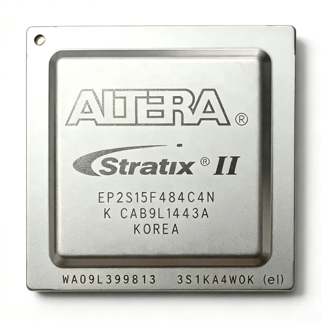

規格比較
| 參數 | EP2S15F484C4 | EP2S15F484I4N |
|---|---|---|
| 品牌 | Intel | Intel |
| 類別 | FPGA & CPLD | FPGA & CPLD |
| 生命週期狀態 | 最後購買 | Obsolete |
| 單價 (USD) | $205.00 | — |
| Family | Stratix II | Stratix II |
| Logic Elements (LEs) | 15,600 | — |
| Adaptive Logic Modules (ALMs) / CLBs | 6,240 | — |
| Embedded Memory (Bits) | 419,328 | — |
| Maximum User I/O | 342 | — |
| DSP Blocks | Yes (integrated multiplier-accumulators) | — |
| 封裝 | 484-FBGA (FBGA-484) | 484-BBGA |
| Package Dimensions | 23 mm x 23 mm | [DATA_NEEDED: package dimensions] |
| Ball Pitch | 1.0 mm | — |
| Process Technology | 90 nm CMOS | — |
| Core Performance | Up to 717 MHz | — |
| Speed Grade | C4 (-4, mid-tier) | — |
| Temperature Grade | Commercial (C): 0 C to +85 C junction | Industrial |
| Supply Voltage (Core) | [DATA_NEEDED: VCCINT nominal] | — |
| I/O Standards Supported | LVDS, LVTTL, LVCMOS, SSTL, HSTL | — |
| External Memory Interface | DDR, DDR2, QDR SRAM | — |
| Configuration Method | Serial/parallel, JTAG | — |
| RoHS 狀態 | Compliant (lead-free FBGA package) | [DATA_NEEDED: RoHS status] |
| Device Type | — | Field Programmable Gate Array (FPGA) |
| Logic Elements | — | 15,600 |
| Embedded Memory | — | 419,328 bits |
| User I/O Pins | — | 342 |
| Configurable Logic Blocks | — | 780 |
| Operating Voltage | — | 1.2 V |
| Terminal Count | — | 484 |
| Terminal Form | — | Ball |
| Package Shape | — | Square |
| 安裝類型 | — | Surface Mount |
| REACH Status | — | [DATA_NEEDED: REACH status] |
| 最大時脈頻率 | — | [DATA_NEEDED: maximum clock frequency] |
| 工作溫度範圍 | — | [DATA_NEEDED: operating temperature range] |