XC7A50T-1CS324I vs XC7A50T-2CSG324I 比較
詳細並排比較 XC7A50T-1CS324I 由 AMD 與 XC7A50T-2CSG324I 由 AMD. 比較關鍵規格、電氣參數、封裝、生命週期狀態、價格與供貨情況,以找出最符合您設計需求的元件。

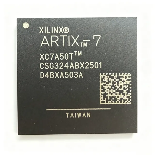
規格比較
| 參數 | XC7A50T-1CS324I | XC7A50T-2CSG324I |
|---|---|---|
| 品牌 | AMD | AMD |
| 類別 | FPGA & CPLD | FPGA & CPLD |
| 生命週期狀態 | 啟用中 | 啟用中 |
| 單價 (USD) | — | $25.45 |
| Device Type | Artix-7 FPGA | — |
| Programmable Logic Cells | 52,160 | — |
| Configurable Logic Blocks | 4,075 | — |
| RAM Bits | 2,764,800 | — |
| Programmable I/O Pins | 210 | — |
| Process Technology | 28 nm | 28nm |
| Core Supply Voltage | 0.95 V to 1.05 V | — |
| Junction Temperature Range | -40°C to 100°C | — |
| 封裝 | 324-CSPBGA | 324-LFBGA, CSPBGA (CSG324) |
| Package Pin or Ball Count | 324 | — |
| 安裝類型 | Surface Mount | Surface Mount |
| Logic Density | 52,160 logic elements | — |
| Device Family | Artix-7 | — |
| FPGA Type | Field-programmable gate array | — |
| Configuration Memory | [DATA_NEEDED: configuration memory specification] | — |
| Block RAM | [DATA_NEEDED: block RAM organization and count] | 2,764,800 bits |
| DSP Resources | [DATA_NEEDED: DSP resource specification] | — |
| Maximum I/O Performance | [DATA_NEEDED: maximum I/O performance] | — |
| RoHS 狀態 | unknown | Compliant |
| REACH Status | unknown | — |
| AEC-Q100 Qualification | not_applicable | — |
| Family | — | Artix-7 |
| Logic Cells | — | 52,160 |
| DSP Slices | — | 120 (DSP48E1) |
| User I/O | — | 210 |
| Core Voltage (VCCINT) | — | 1.0V |
| Speed Grade | — | -2 |
| Temperature Range | — | Industrial (-40°C to +100°C) |
| Configuration Interfaces | — | JTAG, SPI, BPI |
| Clock Management Tiles | — | 5 (MMCM + PLL) |
| I/O Standards | — | LVCMOS, LVDS, HSTL, etc. |