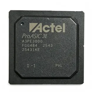
A3P1000-1FG484T - ProASIC3 FPGA, 1M Gates, 300 I/O | Microchip
MPN: A3P1000-1FG484T ✓ 啟用中A3P1000-1FG484T 概覽
An FPGA (Field Programmable Gate Array) is an integrated circuit that can be configured by the customer or designer after manufacturing—hence "field-programmable." Unlike fixed-function ASICs, FPGAs contain an array of programmable logic blocks and a hierarchy of reconfigurable interconnects that allow the same device to implement different digital logic functions. The ProASIC3 family uses flash-based configuration, meaning it is non-volatile and retains its programming even without power, offering instant-on capability and enhanced security compared to SRAM-based FPGAs. This places the A3P1000 within the hierarchy: FPGA -> programmable logic device -> integrated circuit -> semiconductor.
Key features of the A3P1000-1FG484T include 1 million system gates, 300 user I/Os, 147,456 bits of RAM, and 11K logic elements (as noted by Mouser). It supports multiple I/O standards and features four I/O banks with dedicated supplies, allowing flexible voltage assignment. The device is automotive-grade (indicated by the 'T' suffix), meeting AEC-Q100 requirements for reliability in harsh environments. Its flash-based architecture provides low power consumption, high security against reverse engineering, and immunity to configuration bitstream corruption.
Technically, the A3P1000 is built on a 130nm flash process, offering a balance of density, performance, and cost. It includes up to 272 MHz system performance, 1.5V core operation, and supports various memory interfaces. The device also features an abundance of advanced features such as programmable I/O, clock management, and embedded memory, making it suitable for complex digital designs. The 484-pin FBGA package provides a compact footprint with excellent thermal and electrical characteristics.
Typical applications include automotive electronics (e.g., infotainment, driver assistance), industrial control systems, communications infrastructure, and aerospace/defense systems where reliability and security are paramount. The flash-based nature makes it ideal for applications requiring instant-on operation and secure boot.
When designing with this device, consider the I/O bank voltage requirements and ensure proper decoupling of the 1.5V core supply. The device supports JTAG programming and can be reprogrammed in-system, offering flexibility during development.
This page synthesizes distributor pricing, drop-in alternatives, and practical design notes not found in the manufacturer datasheet, providing engineers with a comprehensive resource for evaluating the A3P1000-1FG484T.
直接替換替代品,適用於 A3P1000-1FG484T — 相同封裝,腳位對腳位相容。需重新設計 PCB 的不同封裝零件不列入。
此系列的變體
與下列產品可直接替換的同系列型號: A3P1000-1FG484T (相同外形與佔位) — 差異在於 System Gates, Configuration, Core Voltage, Operating Temperature, Package.
A3P1000-1FG484I
✅ 直接替換📋 參考替代品(不在目錄中)
A3P1000-FG484T
✅ 直接替換📋 參考替代品(不在目錄中)
A3P1000-FG484I
✅ 直接替換📋 參考替代品(不在目錄中)
A3P1000-1FG256T
✅ 直接替換聯絡詢價
查看資料表 →A3P1000L-1FGG484I
✅ 直接替換聯絡詢價
查看資料表 →A3P1000-1FG484T 最大額定值與電氣特性
| Family | ProASIC3 |
| System Gates | 1,000,000 |
| Logic Elements | 11K |
| Number of I/Os | 300 |
| RAM Bits | 147,456 |
| Core Voltage | 1.5 V |
| Maximum System Performance | 272 MHz |
| Technology | 130nm Flash |
| 封裝 | 484-FBGA |
| 安裝類型 | Surface Mount |
| 工作溫度 | -40C to +125C (automotive) |
| I/O Banks | 4 |
| Automotive Grade | Yes (AEC-Q100) |
| RoHS 狀態 | Compliant |
| Configuration | Flash-based, non-volatile |
A3P1000-1FG484T 484-fbga 腳位配置指南
A3P1000-1FG484T(484-fbga 封裝)的腳位配置。 此數位 IC 包含 GPIO、通訊介面(UART、SPI、I2C)與電源腳位。替代腳位功能與配置選項請參閱製造商資料表。對嵌入式系統設計與 PCB 佈局至關重要。

無詳細腳位定義資料: A3P1000-1FG484T.
請參閱 資料表 以查看完整腳位配置。
典型應用
A3P1000-1FG484T 適用於 6 應用s: Automotive Infotainment, Industrial Control Systems, Aerospace and Defense, Communications Infrastructure, Medical Electronics, Test and Measurement.
Automotive Infotainment
The A3P1000-1FG484T is ideal for automotive infotainment systems due to its automotive-grade qualification (AEC-Q100) and extended temperature range (-40C to +125C). With 1M gates and 300 I/Os, it can handle video processing, audio routing, and connectivity interfaces. Its flash-based configuration ensures instant-on operation, which is critical for head-unit boot-up. The device's low power consumption and high reliability make it suitable for the harsh automotive environment. Designers can use its 4 I/O banks to interface with various display and sensor modules, while the 147,456 bits of RAM support buffering for multimedia streams. The non-volatile configuration also provides secure boot, protecting against unauthorized access.
推薦
Industrial Control Systems
In industrial control, the A3P1000-1FG484T provides a reliable, reprogrammable platform for motor control, PLCs, and robotics. Its 1M gates allow implementation of complex control algorithms, while 300 I/Os interface with sensors, actuators, and communication buses. The flash-based FPGA offers instant-on and high security, preventing unauthorized copying of proprietary algorithms. The device operates at 1.5V core, reducing power consumption in always-on industrial equipment. With 272 MHz performance, it can handle real-time processing tasks. The 484-FBGA package is suitable for compact industrial PCBs, and the automotive temperature range ensures operation in factory environments without active cooling. Designers can leverage the 4 I/O banks to support multiple voltage standards, simplifying interface design.
推薦
Aerospace and Defense
The A3P1000-1FG484T is well-suited for aerospace and defense applications due to its flash-based, non-volatile configuration that provides inherent security against reverse engineering and bitstream tampering. With 1M gates and 300 I/Os, it can implement secure communication protocols, radar signal processing, and flight control logic. The device's radiation tolerance (though not explicitly rated) and wide temperature range make it a candidate for avionics. Its instant-on capability is crucial for mission-critical systems that must start immediately. The 484-FBGA package offers a compact footprint for space-constrained avionics boards. Designers can use the 147,456 bits of RAM for data buffering and the 272 MHz performance for high-speed processing. The automotive-grade qualification also implies robust reliability standards.
推薦
Communications Infrastructure
In communications infrastructure, the A3P1000-1FG484T can be used for protocol bridging, packet processing, and interface conversion. Its 1M gates provide ample logic for implementing Ethernet, PCIe, or other protocol stacks, while 300 I/Os connect to PHYs and backplane interfaces. The flash-based FPGA offers low latency and deterministic behavior, essential for real-time communication. With 272 MHz performance, it can handle high-speed data paths. The 147,456 bits of RAM support FIFOs and packet buffers. The device's 1.5V core reduces power in dense networking equipment. The 484-FBGA package is suitable for line cards and switches. The automotive temperature range ensures operation in uncontrolled environments, and the non-volatile configuration allows secure field updates.
推薦
Medical Electronics
The A3P1000-1FG484T is suitable for medical electronics such as patient monitors, imaging systems, and diagnostic equipment. Its flash-based configuration provides secure, non-volatile programming that can be updated in the field, ensuring compliance with evolving medical standards. With 1M gates and 300 I/Os, it can handle sensor interfacing, signal processing, and display control. The device's low power consumption is beneficial for portable medical devices. The 272 MHz performance supports real-time processing of physiological signals. The 484-FBGA package is compact for medical PCBs. The automotive temperature range (-40C to +125C) exceeds typical medical requirements, ensuring reliability. The 147,456 bits of RAM can buffer data for analysis. Designers can use the 4 I/O banks to interface with various analog front-ends.
推薦
Test and Measurement
In test and measurement equipment, the A3P1000-1FG484T provides a flexible platform for implementing custom triggering, data acquisition, and signal analysis. Its 1M gates allow integration of multiple test functions into a single FPGA, reducing board space. With 300 I/Os, it can interface with ADCs, DACs, and external triggers. The flash-based FPGA offers fast configuration and secure IP protection. The 272 MHz performance enables high-speed data capture. The 147,456 bits of RAM support deep buffers for waveform storage. The device's 1.5V core minimizes power in benchtop instruments. The 484-FBGA package is suitable for modular test cards. The automotive temperature range ensures stable operation in lab environments. Designers can use the 4 I/O banks to support various logic levels.
推薦
推薦產品摘要
工程參考資料,適用於 A3P1000-1FG484T — 比較、設計指引及合規資訊。
選型指南
與替代品比較
| 參數 | 本產品 | A3P1000-1FG484I | A3P1000-FG484T | A3P1000-FG484I | A3P1000-1FG256T | A3P1000L-1FGG484I |
|---|---|---|---|---|---|---|
| Package | 484-FBGA | 484-FBGA | 484-FBGA | 484-FBGA | 256-FBGA | 484-FBGA |
| Brand | Microchip Technology | Microchip Technology | Microchip Technology | Microchip Technology | Microchip Technology | Microchip Technology |
| System Gates | 1,000,000 | 1,000,000 | 1,000,000 | 1,000,000 | 1,000,000 | 1,000,000 |
| Number of I/Os | 300 | 300 | 300 | 300 | 177 | 300 |
| RAM Bits | 147,456 | 147,456 | 147,456 | 147,456 | 147,456 | 147,456 |
| Core Voltage | 1.5 V | 1.5 V | 1.5 V | 1.5 V | 1.5 V | 1.5 V |
| Temperature Grade | Automotive (-40C to +125C) | Industrial (-40C to +100C) | Automotive (-40C to +125C) | Industrial (-40C to +100C) | Automotive (-40C to +125C) | Industrial (-40C to +100C) |
主要差異化特點
- Automotive-grade qualification (AEC-Q100) (對比A3P1000-1FG484I)
- Flash-based non-volatile configuration (對比SRAM-based FPGAs)
- High I/O count in 484-FBGA package (對比A3P1000-1FG256T)
設計說明
The A3P1000-1FG484T requires a 1.5V core supply. Use a low-dropout regulator (LDO) or a switching regulator with low ripple to provide this rail. Decouple each VCC pin with a 0.1uF ceramic capacitor and add bulk capacitance (10uF) near the FPGA. The I/O banks have dedicated VCCIBx supplies; ensure each bank's voltage matches the connected I/O standard. Refer to the ProASIC3 datasheet for recommended power-up sequencing.
The 484-FBGA package has a thermal resistance that depends on airflow and PCB design. For high-density designs, ensure adequate copper pour and thermal vias under the package. The automotive temperature range (-40C to +125C) allows operation in harsh environments, but power dissipation must be managed. Estimate junction temperature using the formula Tj = Ta + (theta_JA * P), where P is the total power consumption. For typical designs with 1W dissipation, a theta_JA of 20C/W results in a 20C rise, which is acceptable.
For the 484-FBGA package, use a 4-layer or more PCB with dedicated power and ground planes. Place decoupling capacitors as close to the FPGA pins as possible. Route high-speed signals with controlled impedance and minimize trace lengths. Follow the layout guidelines in the ProASIC3 datasheet, including via placement and ground stitching. Ensure the BGA footprint matches the recommended land pattern to avoid solder joint issues.
合規資訊
Automotive grade (AEC-Q100) per part number suffix 'T'. RoHS compliance indicated by distributor listings. Other compliance details not explicitly stated in provided data.