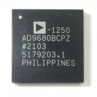
AD9680BCPZ-1000 - Dual 14-Bit 1 GSPS ADC | Analog Devices
MPN: AD9680BCPZ-1000 ✓ 啟用中AD9680BCPZ-1000 概覽
An ADC converts an analog voltage into a digital code for processing, storage, transmission, or measurement. The AD9680 belongs to the high-speed ADC category, combines a pipelined conversion architecture with on-chip input buffers and sample-and-hold circuits, and is intended for communications, instrumentation, radar, and test systems. Its dual-channel architecture allows two analog inputs to be digitized while preserving matched device characteristics.
Key features include 14-bit resolution, dual simultaneous input capability, and operation from a 1.2 V or 2.5 V supply domain as identified in the verified product information. The JESD204B interface enables high-rate digital data transfer between the converter and compatible serializers or processors. The integrated input buffer and sample-and-hold circuit are specifically mentioned by the manufacturer as supporting low power, small size, and ease of use.
At high conversion rates, the ADC must be paired with controlled analog input networks, adequate power delivery, proper clocking, and a digital interface capable of handling the resulting data rate. The two analog channels should use matched routing and impedance considerations to reduce channel-to-channel errors. JESD204B configuration, clock relationships, lane rates, reference voltage, and supported device features must be verified in the manufacturer datasheet before board release.
Typical applications include wireless infrastructure, digital oscilloscopes, spectrum analyzers, radar receivers, communications test equipment, and broadband signal-processing systems. The AD9680 is particularly relevant where multiple high-speed analog channels must be converted into data suitable for high-speed serial transport.
Designers should pay particular attention to the 9 mm by 9 mm LFCSP footprint, exposed-pad thermal management, decoupling, high-speed clock routing, analog input bandwidth, and JESD204B lane configuration. The verified sources identify the component and its major conversion characteristics, but do not provide a complete verified pinout, electrical limit table, lifecycle statement, pricing schedule, or qualified drop-in substitute set.
This page consolidates the verified Analog Devices product information, distributor identifiers, application guidance, and design constraints. It also separates documented facts from missing parameters so that engineers can make sourcing decisions without confusing generic ADC recommendations with verified AD9680BCPZ-1000 data.
直接替換替代品,適用於 AD9680BCPZ-1000 — 相同封裝,腳位對腳位相容。需重新設計 PCB 的不同封裝零件不列入。
此系列的變體
與下列產品可直接替換的同系列型號: AD9680BCPZ-1000 (相同外形與佔位) — 差異在於 Package, Supply Voltage, Sampling Rate, Resolution, Operating Temperature.
AD9680BCPZ-1000
✅ 直接替換聯絡詢價
查看資料表 →AD9680BCPZ-1000 最大額定值與電氣特性
| Product Type | Dual analog-to-digital converter |
| 解析度 | 14 bit |
| Number of Inputs | 2 inputs |
| Conversion Architecture | Pipelined |
| Maximum Sampling Rate | 1 GSPS for AD9680BCPZ-1000 |
| Family Sampling Rates | 1.25 GSPS, 1 GSPS, 820 MSPS, 500 MSPS |
| 介面 | JESD204B |
| On-Chip Buffer | Yes |
| Sample-and-Hold Circuit | Yes |
| 供應電壓 | 1.2 V / 2.5 V |
| 封裝 | 64-LFCSP (9 mm x 9 mm) |
| 安裝類型 | Surface Mount |
| Channel Configuration | Dual, 2-channel |
| Sampling Circuit | On-chip sample-and-hold |
| Data Transfer Standard | JESD204B |
AD9680BCPZ-1000 64-lfcsp (9 mm x 9 mm) 腳位配置指南
AD9680BCPZ-1000(64-lfcsp (9 mm x 9 mm) 封裝)的腳位配置。 此類比元件具有輸入、輸出與電源腳位。偏移歸零、補償與致能腳位配置請參閱製造商資料表。適用於訊號調理與放大器電路。

無詳細腳位定義資料: AD9680BCPZ-1000.
請參閱 資料表 以查看完整腳位配置。
典型應用
AD9680BCPZ-1000 適用於 6 應用s: Wireless Communications Infrastructure, Digital Oscilloscopes and Signal Analyzers, Radar and Wideband Receiver Systems, Communications Test Equipment, Spectrum Analyzer Front Ends, High-Speed Data Acquisition.
Wireless Communications Infrastructure
The AD9680BCPZ-1000 fits wireless infrastructure receivers that need two high-speed analog channels and digital conversion into a JESD204B link. Its verified 14-bit resolution, 1 GSPS ordering-option rate, integrated input buffer, and integrated sample-and-hold circuit reduce the number of separate front-end acquisition stages. A practical receiver would place matched filtering and gain ahead of the two analog inputs, then route the converter output through a JESD204B-capable FPGA or ASIC. The engineer must verify input bandwidth, clocking, lane rate, synchronization, reference requirements, and thermal performance against the actual radio architecture.
推薦
Digital Oscilloscopes and Signal Analyzers
AD9680BCPZ-1000 is applicable to high-speed measurement instruments that capture two related analog signals for real-time analysis. The dual 14-bit pipeline can support synchronized acquisition, while the 1 GSPS option provides a substantial sample rate for bandwidth-limited or wideband intermediate-frequency measurements. Its JESD204B output can connect the converter to a high-speed processing fabric instead of relying only on parallel data capture. Instrument designers still need to establish analog bandwidth, gain distribution, clock jitter, memory throughput, calibration, and trigger synchronization before selecting the part for a particular measurement class.
推薦
Radar and Wideband Receiver Systems
The AD9680BCPZ-1000 can be used in radar or wideband receiver signal chains when the system requires digitizing dual channels at a high conversion rate. The 14-bit conversion resolution and 1 GSPS ordering-option rate are useful for capturing intermediate-frequency or digitized receiver outputs, while the integrated buffer and sample-and-hold circuitry support compact analog implementations. The JESD204B interface can reduce parallel data routing by transporting converter data to suitable digital logic. Radar designers must account for RF-to-IF conversion, anti-alias filtering, clock jitter, channel skew, thermal rise, and deterministic firmware or FPGA calibration.
推薦
Communications Test Equipment
The AD9680BCPZ-1000 is well suited to communications test equipment that evaluates modulated or wideband signals with two synchronized acquisition channels. The 1 GSPS option and JESD204B interface support high-throughput capture into programmable logic, while 14-bit resolution supports measurement chains where quantization noise is relevant. A practical instrument would combine the ADC with controlled RF or IF conditioning, a low-jitter clock source, and a data-processing section. Calibration, input range, bandwidth, channel matching, jitter performance, and firmware-supported modulation analysis must be verified before production use.
推薦
Spectrum Analyzer Front Ends
The AD9680BCPZ-1000 may support spectrum-analyzer front ends that require simultaneous conversion of two RF or IF paths. Its dual-channel architecture helps preserve comparison measurements, while its high-rate pipelined conversion and JESD204B output can feed a processor capable of FFT and channel analysis. The converter is not a complete analyzer front end: designers still need RF filtering, gain control, local-oscillator or clock generation, anti-alias filtering, calibration, and thermal design. Confirm the exact analog input range, bandwidth, SNR, SFDR, and reference requirements in the AD9680 datasheet.
推薦
High-Speed Data Acquisition
The AD9680BCPZ-1000 is appropriate for high-speed data-acquisition systems that need two 14-bit channels and a compact high-speed converter package. The 1 GSPS ordering-option rate and on-chip input buffer support acquisition of waveforms or intermediate signals, while JESD204B provides a structured high-speed digital interface for downstream logic. The system designer should select external analog bandwidth, gain, input termination, clocking, and memory or FPGA resources to match the intended sample rate. Because the supplied data does not include verified power, SNR, SFDR, and temperature limits, those values must be established before determining thermal headroom.
推薦
工程參考資料,適用於 AD9680BCPZ-1000 — 比較、設計指引及合規資訊。
選型指南
與替代品比較
| 參數 | 本產品 | AD9680BCPZ-1000 |
|---|---|---|
| Package | 64-LFCSP (9 mm x 9 mm) | 64-LFCSP (9 mm x 9 mm) |
| Brand | Analog Devices | Analog Devices |
| Resolution | 14 bit | 14 bit |
| Input Channels | 2 | 2 |
| Sampling Rate | 1 GSPS | 1 GSPS |
| Architecture | Pipelined | Pipelined |
| Digital Interface | JESD204B | JESD204B |
| Supply Designation | 1.2 V / 2.5 V | 1.2 V / 2.5 V |
| On-Chip Buffer | Yes | Yes |
| Sample-and-Hold | Yes | Yes |
主要差異化特點
- Dual 14-bit acquisition in one converter (對比AD9680BCPZ-1000)
- High-speed JESD204B integration (對比AD9680BCPZ-1000)
- Integrated acquisition front end (對比AD9680BCPZ-1000)
設計說明
Use the official AD9680 package drawing and complete datasheet to place the 64-LFCSP footprint, exposed pad, analog inputs, supplies, clock pins, and JESD204B interface. Keep analog input and clock routing short, controlled, and referenced to a solid ground plane. Because the verified data does not provide the complete pinout, do not release a layout from package dimensions alone. Confirm via the manufacturer’s recommended decoupling and reference circuitry before fabrication.
Treat the two analog inputs, sampling clock, reference network, and JESD204B links as separate high-speed domains. Use matched input paths and controlled impedance, minimize discontinuities, and isolate noisy digital return currents from sensitive analog areas. The 1 GSPS option requires careful attention to clock jitter, edge rate, insertion loss, crosstalk, and impedance discontinuities. Validate the complete layout with simulation and measurements because verified AD9680BCPZ-1000 SNR, SFDR, bandwidth, and jitter values were not supplied.
The AD9680BCPZ-1000 is a high-speed dual ADC in a 9 mm by 9 mm LFCSP package, so exposed-pad heat spreading is important. Use the manufacturer’s land pattern and thermal guidance, provide low-impedance supply and ground connections, and assess junction temperature at the intended ambient and sampling rate. Do not calculate a final thermal limit from an unverified power value; obtain the datasheet power dissipation and package thermal data first, then apply the actual board thermal resistance.
Do not assume that the AD9680 family’s 1.25 GSPS capability applies automatically to AD9680BCPZ-1000, or that any ADC with the same resolution can replace it. The -1000 ordering option is verified at 1 GSPS, while the broader family supports multiple rates. Likewise, same-package appearance is insufficient for replacement: verify all 64 pins, JESD204B lane behavior, clock requirements, supply sequencing, reference voltage, analog range, and timing before substitution.
合規資訊
The supplied verified sources identify the manufacturer and product but do not provide extracted RoHS, REACH, AEC-Q100, lead-free, halogen-free, or conflict-minerals statements. No compliance claim is inferred.