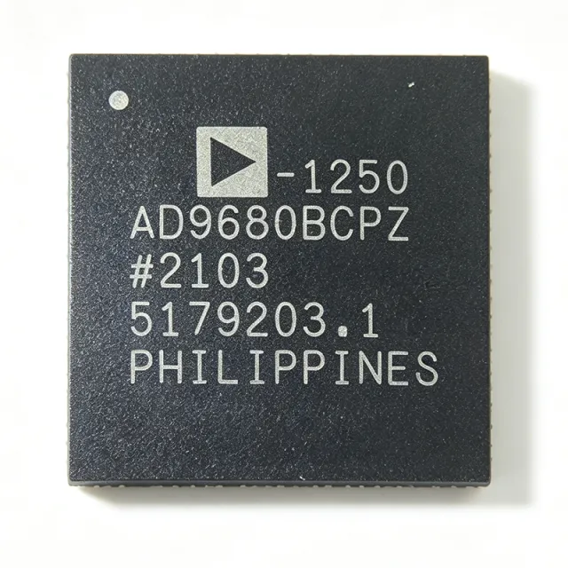
AD9680BCPZ-1250 - Dual 14-Bit 1.25 GSPS ADC JESD204B | Analog Devices
MPN: AD9680BCPZ-1250 ✓ 啟用中AD9680BCPZ-1250 概覽
An ADC (analog-to-digital converter) is a mixed-signal semiconductor device that converts continuous analog waveforms into discrete digital data for processing by FPGAs, DSPs, or other digital logic. Within the signal-chain hierarchy, the AD9680 belongs to the RF-sampling, high-speed pipelined ADC class, sitting upstream of digital processing elements such as the Intel/Altera and Xilinx FPGAs commonly paired with it over JESD204B serial links.
Key features include dual 14-bit conversion cores running at up to 1.25 GSPS per channel, an on-chip buffer and sample-and-hold circuit optimized for low power, small size, and ease of use, and a JESD204B serial data output that dramatically reduces pin count versus parallel LVDS/CMOS interfaces. Speed-grade variants of the same family offer 500 MSPS, 820 MSPS, 1 GSPS, and 1.25 GSPS, allowing a single PCB footprint to serve multiple bandwidth tiers.
Technically, the pipelined architecture uses cascaded sub-ranging stages with digital error correction, enabling high sample rates while maintaining 14-bit resolution. The integrated input buffer eases drive requirements for wideband amplifiers or passive networks, and on-chip digital functions (DDC-style processing blocks per the ADI product family) reduce FPGA resource load in digital pre-distortion and observation-receiver designs.
Typical applications include wideband software-defined radios, 3G/4G/5G cellular base-station receivers, digital pre-distortion (DPD) observation channels, and test-and-measurement instrumentation requiring GHz-class analog input bandwidth.
Design consideration: operate within the recommended clock and supply architecture, and budget power and thermal performance for the 64-LFCSP thermally enhanced package, since multi-gigasample operation drives the dominant portion of power dissipation.
This page synthesizes distributor pricing and availability, drop-in same-family speed-grade alternatives, and practical design guidance not consolidated in the manufacturer datasheet. Pricing shown is as of 2026-09-05.
直接替換替代品,適用於 AD9680BCPZ-1250 — 相同封裝,腳位對腳位相容。需重新設計 PCB 的不同封裝零件不列入。
此系列的變體
與下列產品可直接替換的同系列型號: AD9680BCPZ-1250 (相同外形與佔位) — 差異在於 Package, Resolution, RoHS Status.
AD9680BCPZ-500
聯絡詢價
查看資料表 →AD9680BCPZRL7-1000
聯絡詢價
查看資料表 →AD9680BCPZ-1000
聯絡詢價
查看資料表 →AD9680BCPZ-820
📋 參考替代品(不在目錄中)
AD9680BCPZRL7-820
📋 參考替代品(不在目錄中)
AD9680BCPZ-1250 最大額定值與電氣特性
| 解析度 | 14 bit |
| Number of Channels | 2 |
| Sampling Rate (Max) | 1.25 GSPS |
| Architecture | Pipelined |
| Analog Input Bandwidth | Up to 2 GHz |
| 介面類型 | JESD204B serial output |
| Input Buffer | On-chip buffer and sample-and-hold |
| 封裝 | 64-LFCSP (9 mm x 9 mm) |
| 安裝類型 | Surface Mount |
| Family Speed Grades | 500 MSPS / 820 MSPS / 1 GSPS / 1.25 GSPS |
| Analog Input Type | Differential |
| RoHS 狀態 | RoHS Compliant (per distributor listings) |
AD9680BCPZ-1250 64-lfcsp (9 mm x 9 mm) 腳位配置指南
AD9680BCPZ-1250(64-lfcsp (9 mm x 9 mm) 封裝)的腳位配置。 此類比元件具有輸入、輸出與電源腳位。偏移歸零、補償與致能腳位配置請參閱製造商資料表。適用於訊號調理與放大器電路。

無詳細腳位定義資料: AD9680BCPZ-1250.
請參閱 資料表 以查看完整腳位配置。
典型應用
AD9680BCPZ-1250 適用於 6 應用s: 5G Base Station Receiver, Digital Pre-Distortion Observation Receiver, Software-Defined Radio, Test and Measurement Instrumentation, Phased Array Radar and Electronic Warfare, Industrial Wideband Data Acquisition.
5G Base Station Receiver
The AD9680BCPZ-1250 fits 5G massive-MIMO and macro-cell receivers because its 1.25 GSPS sampling rate delivers roughly 625 MHz of Nyquist bandwidth, enough to capture wide 5G NR carrier aggregations directly at IF or RF, while the 2 GHz analog input bandwidth supports high IF architectures that eliminate mixer stages. The dual 14-bit channels let a single device digitize two antennas or a main-plus-observation path, halving converter count. Data exits over JESD204B serial lanes that connect directly to FPGA transceivers, providing the deterministic latency and multi-chip synchronization those beamforming systems require. Engineers should budget power and thermal margin in the 64-LFCSP package at full 1.25 GSPS clock rates.
推薦
Digital Pre-Distortion Observation Receiver
In DPD observation loops, the AD9680BCPZ-1250 digitizes the feedback path of a power amplifier so DSP algorithms can linearize wideband, multi-carrier transmit signals. Its 1.25 GSPS rate captures PA output distortion products across hundreds of MHz of occupied bandwidth, and the 2 GHz analog input handles the high LO-derived IFs typical of feedback couplers. The on-chip buffer and sample-and-hold ease interfacing to passive feedback networks per Analog Devices design guidance, and the JESD204B link moves samples to the baseband FPGA at low pin count. Since observation paths run continuously, many designs use the lower-cost AD9680BCPZ-1000 grade when bandwidth analysis permits, trading 20% sample rate for power and cost savings on the same footprint.
推薦
Software-Defined Radio
Wideband SDR platforms benefit from the AD9680BCPZ-1250's direct-RF sampling capability: sampling at 1.25 GSPS with a 2 GHz analog input bandwidth allows digitization of HF-through-S-band signals without multiple mixer stages, simplifying the RF front end and improving flexibility across waveforms. The dual channels support diversity reception or simultaneous main/monitor paths, and JESD204B output integrates cleanly with the FPGA-centric architecture of modern SDR. Designers should place attention on clock phase noise, because GSPS-class sampling converts clock jitter directly into SNR degradation at high input frequencies; a low-jitter clock source and careful analog input matching preserve the 14-bit dynamic range the converter offers.
推薦
Test and Measurement Instrumentation
Oscilloscope front ends, spectrum analyzers, and recorders use the AD9680BCPZ-1250 where GHz-class acquisition bandwidth and 14-bit resolution are both required. The 1.25 GSPS dual cores enable interleaved or dual-channel capture of fast edges and wideband modulations, while the integrated buffer and sample-and-hold per Analog Devices simplify driving from high-bandwidth attenuator/amplifier chains. The JESD204B serial output keeps the digital interface compact inside dense instruments and supports the deterministic trigger-to-data latency these products specify. Instrument makers should implement the recommended power-supply filtering and ground scheme for the 64-LFCSP exposed pad, since spurious performance in interleaved architectures depends heavily on supply and clock cleanliness.
推薦
Phased Array Radar and Electronic Warfare
Multi-channel radar and EW receivers pair the AD9680BCPZ-1250 with the ADAR1000 X/Ku-band beamformer: the ADC's 1.25 GSPS sampling and 2 GHz input bandwidth digitize wideband chirp and threat waveforms directly at IF, while JESD204B multi-chip synchronization keeps dozens of channels coherent across the array. The dual channels reduce converter count per element pair, important where aperture channel density dominates board area. The shared 64-LFCSP footprint across AD9680 speed grades lets one receiver design scale from 500 MSPS trainer units to 1.25 GSPS operational units without PCB respin. Designers must validate the die-revision PCN 16_0107 implications for long-production military programs.
推薦
Industrial Wideband Data Acquisition
High-end industrial systems - RF impairment test sets, coherent optical modulation analyzers, and wideband vibration/acoustic array systems - use the AD9680BCPZ-1250 when conventional 1-GSPS-class converters lack bandwidth. The dual 14-bit channels provide simultaneous correlated acquisition, the on-chip buffer relaxes analog drive design in modular instruments, and the JESD204B output plugs into standard FPGA development platforms built around Intel MAX 10 and Cyclone 10 devices. For cost-optimized industrial variants where 250 MHz Nyquist bandwidth suffices, the pin-compatible AD9680BCPZ-500 (stocked on XAIPART) drops system power and cost while preserving the PCB layout. Verify operating temperature requirements against the datasheet for conduction-cooled industrial enclosures.
推薦
推薦產品摘要
工程參考資料,適用於 AD9680BCPZ-1250 — 比較、設計指引及合規資訊。
選型指南
與替代品比較
| 參數 | 本產品 | AD9680BCPZ-1000 | AD9680BCPZ-820 | AD9680BCPZ-500 | AD9680BCPZRL7-820 |
|---|---|---|---|---|---|
| Package | 64-LFCSP (9x9 mm) | 64-LFCSP (9x9 mm) - same | 64-LFCSP (9x9 mm) - same | 64-LFCSP (9x9 mm) - same | 64-LFCSP (9x9 mm) - same |
| Brand | Analog Devices | Analog Devices | Analog Devices | Analog Devices | Analog Devices |
| Resolution | 14 bit | 14 bit | 14 bit | 14 bit | 14 bit |
| Max Sampling Rate | 1.25 GSPS | 1 GSPS | 820 MSPS | 500 MSPS | 820 MSPS |
| Channels | 2 | 2 | 2 | 2 | 2 |
| Interface | JESD204B | JESD204B | JESD204B | JESD204B | JESD204B |
主要差異化特點
- Fastest speed grade in the AD9680 family (對比AD9680BCPZ-1000)
- Dual 14-bit cores with JESD204B output in a compact 9x9 mm footprint (對比AD9680BCPZ-820)
- Lower-power substitution path on identical footprint (對比AD9680BCPZ-500)
設計說明
At 1.25 GSPS, aperture and clock jitter dominate SNR at high analog input frequencies. Estimated: total jitter contributions from the encode clock should be kept in the sub-100 fs region for wideband inputs near 1 GHz, since SNR_jitter ≈ -20*log10(2*pi*fin*tjitter). Use a low-phase-noise clock source and differential clock distribution per the Analog Devices AD9680 datasheet clocking recommendations, and keep clock and analog input return paths separated on the PCB.
The 64-LFCSP (9x9 mm) package has an exposed die-attach pad that must be soldered to a continuous ground plane with a via array for thermal and electrical performance. Place the JESD204B lanes as controlled-impedance differential pairs with length matching per the JESD204B standard timing budget, and follow the ADI reference design land pattern exactly. Decouple all supply domains with low-ESR ceramics placed directly at the pins; the datasheet power-supply architecture table specifies per-domain decoupling values.
Power dissipation scales strongly with sample rate across the AD9680 family. Estimated: if the -1250 grade dissipates P watts at 1.25 GSPS, the -500 grade on the same footprint runs proportionally lower, so systems whose Nyquist requirement is 250 MHz can cut converter power materially by selecting AD9680BCPZ-500 without respinning the board. Always compute junction temperature from the datasheet theta-JA for your airflow condition before finalizing the thermal design; exact typical power figures were not in the source data for this page and should be read from the current datasheet revision (note PCN 16_0107 die change).
Verify the die revision on incoming lots: Analog Devices PCN 16_0107 (Dec 9, 2016) implemented a die revision and data sheet change for the AD9680-500/820/1000/1250 grades. Systems qualified against pre-PCN datasheet revisions or specific date codes must re-validate. Also confirm JESD204B lane mapping and sync (SYSREF) implementation against the current datasheet rather than copied designs, and do not assume cross-brand 'equivalent' GSPS ADCs are drop-in - package and JESD204B lane order generally differ.
合規資訊
RoHS compliance per DigiKey/Mouser distributor listings for AD9680BCPZ-1250. No AEC-Q100 qualification indicated. REACH and halogen-free status not stated in provided data.






