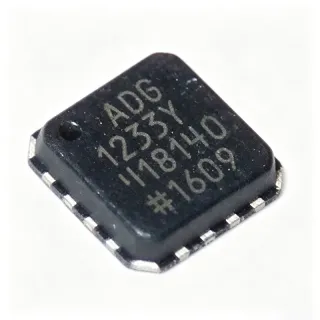
ADF4154BCPZ-RL7 - 4 GHz Fractional-N PLL Synthesizer | Analog Devices
MPN: ADF4154BCPZ-RL7 ✓ 啟用中ADF4154BCPZ-RL7 概覽
A fractional-N frequency synthesizer is a phase-locked-loop device that generates precise local-oscillator signals for RF transmitters and receivers. The ADF4154 combines a low-noise digital phase-frequency detector, a precision charge pump, a programmable reference divider, and a sigma-delta fractional interpolator. This architecture supports integer and fractional division ratios while preserving stable phase locking across programmable output frequencies.
The principal operating features include RF bandwidth to 4 GHz, a 2.7 V to 3.3 V power supply, programmable charge-pump currents, a separate VP tuning-voltage supply, digital lock detection, and power-down mode. The dual 4/5 and 8/9 prescalers extend the usable integer-N range, while the sigma-delta fractional interpolator enables fine frequency synthesis for wireless transceiver architectures.
The 3-wire serial interface provides a compact control path for programming divider ratios, prescaler selection, charge-pump settings, and power state. The device is designed for direct PCB integration where RF routing, grounding, decoupling, and exposed-pad thermal management are critical. Its separate VP connection allows the tuning-voltage range to be extended beyond the constraints imposed by the main supply when appropriate external circuitry and voltage limits are used.
Typical applications include wireless receiver and transmitter local oscillators, microwave up-converters and down-converters, frequency-agile test equipment, RF signal generators, radar-related signal chains, and industrial RF communication systems. In these systems, the synthesizer supplies a programmable reference for mixers or other RF conversion stages.
PCB design should minimize RF trace loss, maintain a continuous ground reference beneath the exposed pad, and place supply and decoupling connections close to their associated pins. Loop-filter components and the reference input should be positioned to avoid noisy digital-control coupling. The manufacturer datasheet is the controlling reference for register programming, pin assignments, recommended application circuits, and absolute operating limits.
This product page consolidates the verified device identity, package information, manufacturer documentation, operating features, sourcing guidance, and practical integration considerations. It also distinguishes true pin-compatible family alternatives from parts that require different packages or different synthesizer architectures, helping engineers evaluate replacement options without implying that every similar PLL is a drop-in replacement.
直接替換替代品,適用於 ADF4154BCPZ-RL7 — 相同封裝,腳位對腳位相容。需重新設計 PCB 的不同封裝零件不列入。
此系列的變體
與下列產品可直接替換的同系列型號: ADF4154BCPZ-RL7 (相同外形與佔位) — 差異在於 Package, Charge Pump, Charge-Pump Current, Device Type, Lock Detect.
ADF4153BCPZ-RL7
✅ 直接替換聯絡詢價
查看資料表 →ADF4157BCPZ-RL7
✅ 直接替換聯絡詢價
查看資料表 →ADF4154BCPZ-RL7 規格
| Device Type | Fractional-N frequency synthesizer (RF) IC |
| Maximum RF Frequency | 4 GHz |
| Minimum RF Frequency | 200 MHz |
| Power-Supply Range | 2.7 V to 3.3 V |
| Dual-Modulus Prescaler | 4/5 and 8/9 |
| Programmable Charge-Pump Currents | 2 selectable settings |
| Control Interface | 3-wire serial interface |
| Reference Input Logic | CMOS |
| 輸出類型 | Clock |
| Number of Circuits | 1 |
| Input-to-Output Ratio | 2:1 |
| Differential Output | No |
| Lock Detection | Digital |
| Power-Down Mode | Supported |
| Tuning Supply | Separate VP connection |
| 封裝 | 20-WFQFN exposed-pad chip-scale package |
| 安裝類型 | Surface mount |
ADF4154BCPZ-RL7 20-wfqfn exposed-pad chip-scale package 腳位配置指南
ADF4154BCPZ-RL7(20-wfqfn exposed-pad chip-scale package 封裝)的腳位配置。 腳位編號、功能與連接圖定義於製造商資料手冊中。請參閱該手冊以取得確切的封裝尺寸與焊接指引。

無詳細腳位定義資料: ADF4154BCPZ-RL7.
請參閱 資料表 以查看完整腳位配置。
典型應用
ADF4154BCPZ-RL7 適用於 6 應用s: Wireless Receiver Local Oscillator, Wireless Transmitter Up-Converter, Microwave Down-Converter, RF Signal Generator, Frequency-Swept Test Equipment, Industrial RF Communication Module.
Wireless Receiver Local Oscillator
The ADF4154BCPZ-RL7 fits a programmable receiver local-oscillator block that must cover RF channels approaching the device's 4 GHz upper bandwidth. Its 4/5 and 8/9 dual-modulus prescalers support the required integer division range, while the sigma-delta fractional interpolator enables fine channel spacing. The 3-wire interface minimizes control wiring, and digital lock detect supports system-level monitoring. A production design should verify reference phase noise, loop bandwidth, lock margin, and RF output power across the complete channel plan.
推薦
Wireless Transmitter Up-Converter
In a transmitter up-conversion path, the ADF4154BCPZ-RL7 can generate a programmable local-oscillator signal for driving a mixer or subsequent RF stage. Its RF bandwidth to 4 GHz accommodates high-band transmitter plans, while programmable charge-pump currents allow the loop filter to be tuned for phase noise and acquisition performance. The separate VP connection supports extended tuning-voltage designs. Engineers should verify spur performance, output isolation, and compliance with the final transmitter mask using the complete reference and loop-filter design.
推薦
Microwave Down-Converter
The ADF4154BCPZ-RL7 is suitable for the programmable oscillator driving a microwave down-converter or receiver mixer. Operation to 4 GHz provides substantial tuning range for microwave links, while the fractional-N architecture supports precise channel selection. The 3-wire control interface reduces the logic-routing burden in compact RF modules. Layout must preserve short RF paths and a low-impedance ground plane, and the loop filter must be evaluated for both phase noise and the acquisition time required when changing channels.
推薦
RF Signal Generator
The ADF4154BCPZ-RL7 can form the programmable frequency source in an RF signal-generator architecture where accurate channel selection and repeatable phase locking are required. Its programmable prescaler, charge-pump currents, and fractional interpolator permit the loop design to be adapted to different output frequencies. The digital lock-detect feature can supervise acquisition, while power-down mode supports controlled operating states. For laboratory-grade results, reference phase noise, RF output matching, and filter-component tolerances must be evaluated alongside the synthesizer.
推薦
Frequency-Swept Test Equipment
The fractional-N capability of the ADF4154BCPZ-RL7 supports programmable swept or stepped excitation for RF test systems. The 4 GHz maximum RF bandwidth permits high-frequency test points, and the serial interface allows a controller to update divider and tuning parameters efficiently. Digital lock detect provides a signal that a test sequencer can use before accepting a measurement. Switching-time targets depend on loop bandwidth, reference frequency, prescaler choice, and filter design, so they should be measured rather than inferred from interface speed alone.
推薦
Industrial RF Communication Module
The ADF4154BCPZ-RL7 can provide a compact programmable oscillator for industrial RF communication equipment requiring channel selection and stable phase lock. The 20-WFQFN exposed-pad package supports dense RF board layouts, and the 3-wire interface minimizes control-signal count. Industrial equipment designers should account for temperature-dependent loop behavior, reference-source quality, and conducted or radiated emissions from the RF output network. The digital lock-detect output also helps the host controller distinguish an unlocked channel from an operating fault.
推薦
推薦產品摘要
工程參考資料,適用於 ADF4154BCPZ-RL7 — 比較、設計指引及合規資訊。
選型指南
與替代品比較
| 參數 | 本產品 | ADF4153BCPZ-RL7 | ADF4157BCPZ-RL7 |
|---|---|---|---|
| Package | 20-WFQFN exposed-pad chip-scale package | 20-WFQFN exposed-pad chip-scale package | 20-WFQCN exposed-pad chip-scale package |
| Brand | Analog Devices | Analog Devices | Analog Devices |
| Synthesizer Architecture | Fractional-N | Fractional-N | Fractional-N |
| Control Interface | 3-wire serial interface | 3-wire serial interface | 3-wire serial interface |
| Lock Detection | Digital | Digital | Digital |
| Power-Down Mode | Supported | Supported | Supported |
| Pin Compatibility | ADF4154 family pin-compatible reference | ADF4154 datasheet identifies the ADF4153 as pin-compatible | Pin-compatible family construction documented in comparison data |
| Output Type | Clock | Clock | Clock |
主要差異化特點
- Higher upper RF frequency than the ADF4153 family alternative (對比ADF4153BCPZ-RL7)
- Documented family pin compatibility supports PCB reuse (對比ADF4153BCPZ-RL7)
- Programmable dual-modulus prescaler supports flexible RF division (對比ADF4157BCPZ-RL7)
- Separate VP connection supports extended tuning-voltage design (對比ADF4153BCPZ-RL7)
設計說明
Use the manufacturer package drawing to define the 20-WFQFN land pattern and exposed-pad connection. Keep the RF output route short and away from the digital write-data line and reference-clock path. Provide a continuous ground reference under the device, place bypass capacitors at the supply pins, and route the charge-pump and loop-filter connections away from high-current switching nodes to reduce coupling and phase-noise degradation.
Do not select a family alternative from package appearance alone. The ADF4153 has a lower upper-frequency capability, while the ADF4157 has a different upper-frequency specification; either substitution must be checked against the complete frequency plan. Also review register behavior, required output-buffer configuration, reference-input requirements, and loop-filter recalculation before treating either part as a production replacement.
Separate the AVDD supply-decoupling network from noisy digital and RF return currents. Use the manufacturer-recommended capacitor values and placement around the device, and keep the exposed pad thermally and electrically connected as directed. The VP connection is not a substitute for the main supply: its allowed voltage and decoupling depend on the selected charge-pump and tuning-voltage implementation, so verify those limits before energizing the circuit.
Design the reference input as a clean, controlled clock source because reference phase noise and spurs propagate through the fractional-N loop. Keep the reference trace short, provide a defined return path, and isolate it from the 3-wire programming signals. After assembly, evaluate reference spurs, fractional-N spur behavior, lock margin, and phase noise at the intended output frequency rather than relying only on the synthesizer's maximum-frequency rating.
合規資訊
No explicit RoHS, REACH, lead-free, halogen-free, or conflict-minerals status was established for the exact ordering code. AEC-Q100 status is not applicable because this is not presented as an automotive-qualified ordering code.