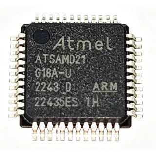
ATMEGA3209-AUR - 20MHz 32KB AVR MCU, TQFP-48 | Microchip
MPN: ATMEGA3209-AUR ✓ 啟用中ATMEGA3209-AUR 概覽
A microcontroller (MCU) is a single-chip computer containing a processor core, program memory, data memory, and programmable I/O peripherals. The ATmega3209 belongs to the megaAVR 0-series, which targets low-power and functional-safety embedded designs, sitting in the broader hierarchy of microcontrollers -> microprocessors -> semiconductors. Compared to traditional AVR (e.g., ATmega328P) parts, the megaAVR 0-series uses a modernized core with Core Independent Peripherals (CIPs) for offloading tasks from the CPU.
Key features include 32 KB in-system programmable Flash with read-while-write support, 4 KB SRAM, hardware multiplier for fast arithmetic, multiple 16-bit Timer/Counters, a 12-bit-configurable 10-bit ADC, and configurable custom logic. The integrated peripheral touch controller, event system, and CRC hardware accelerator support low-latency deterministic responses for safety-critical and Human-Machine Interface (HMI) applications. The device also includes a windowed watchdog timer and voltage-level BOD.
Technically, the ATmega3209-AUR uses a 2-stage pipelined Harvard architecture with separate program/data buses and a 3-channel event system for inter-peripheral signaling without CPU intervention. Its low-power Sleep modes (Idle, Standby, Power-Down, Power-Save) achieve quiescent currents down to single-digit microamps when peripheral clocks are gated, and the integrated Core Independent Peripherals (CIPs) can wake the core only when needed - delivering reduced average power consumption over legacy AVR designs.
Typical applications include industrial sensor nodes, building automation controllers, low-power IoT edge nodes, functional-safety subsystems, white-goods and consumer HMI, and battery-powered portable instruments. Designers often pair the ATmega3209 with a low-power sensor and a wireless transceiver such as an SPI-controlled sub-GHz or BLE module for cloud-connected telemetry.
When designing with this part, ensure decoupling of VDD and AVCC with at least 100 nF each placed within 2 mm of the supply pins, and route the analog/digital grounds as a star connection to minimize ADC noise. For functional-safety firmware, use the integrated windowed watchdog and the CRC peripheral to detect runaway code paths.
This page synthesizes distributor pricing, same-package drop-in alternatives, and practical design notes not found in the manufacturer datasheet alone, helping engineers shorten the BOM selection and PCB layout phases for ATmega3209-based designs.
直接替換替代品,適用於 ATMEGA3209-AUR — 相同封裝,腳位對腳位相容。需重新設計 PCB 的不同封裝零件不列入。
此系列的變體
與下列產品可直接替換的同系列型號: ATMEGA3209-AUR (相同外形與佔位) — 差異在於 Core Processor, Operating Temperature, Peripherals, Series, Packaging.
ATMEGA4809-AUR
✅ 直接替換聯絡詢價
查看資料表 →ATMEGA3208-AUR
✅ 直接替換聯絡詢價
查看資料表 →ATMEGA1609-AUR
✅ 直接替換聯絡詢價
查看資料表 →ATMEGA4808-AUR
✅ 直接替換聯絡詢價
查看資料表 →ATMEGA808-AUR
✅ 直接替換聯絡詢價
查看資料表 →ATMEGA3209-AUR 最大額定值與電氣特性
| Core Processor | AVR 8-bit |
| Core Size | 8-Bit |
| Series | megaAVR 0 |
| Maximum Clock Speed | 20 MHz |
| Program Memory (Flash) | 32 KB |
| SRAM | 4 KB |
| EEPROM | 256 bytes |
| Supply Voltage (VDD) | 1.8 V to 5.5 V |
| 工作溫度 | -40°C to +85°C |
| 封裝 | 48-pin TQFP (7x7 mm) |
| 安裝類型 | Surface Mount (Tape & Reel) |
| ADC | 10-bit, multiple channels |
| Connectivity | I²C, SPI, UART/USART |
| Peripherals | Brown-out Detect, Watchdog, PWM, Timer |
| Hardware Multiplier | Yes |
| RoHS 狀態 | Compliant |
| MSL 等級 | 3 |
ATMEGA3209-AUR 腳位配置
| 腳位 1 | PA6 — Port A bit 6 (GPIO/ADC) |
| 腳位 2 | PA7 — Port A bit 7 (GPIO/ADC) |
| 腳位 3 | AGND — Analog ground |
| 腳位 4 | AVCC — Analog supply voltage |
| 腳位 5 | VDD — Digital supply voltage |
| 腳位 6 | GND — Digital ground |
| 腳位 7 | PC0 — Port C bit 0 (GPIO) |
| 腳位 8 | PC1 — Port C bit 1 (GPIO) |
| 腳位 9 | PC2 — Port C bit 2 (GPIO) |
| 腳位 10 | PC3 — Port C bit 3 (GPIO) |
| 腳位 11 | UPDI — Unified Program and Debug Interface |
| 腳位 12 | PD0 — Port D bit 0 (GPIO) |
| 腳位 13 | PD1 — Port D bit 1 (GPIO) |
| 腳位 14 | PD2 — Port D bit 2 (GPIO) |
| 腳位 15 | PD3 — Port D bit 3 (GPIO) |
| 腳位 16 | PD4 — Port D bit 4 (GPIO) |
| 腳位 17 | PD5 — Port D bit 5 (GPIO) |
| 腳位 18 | PD6 — Port D bit 6 (GPIO) |
| 腳位 19 | PD7 — Port D bit 7 (GPIO) |
| 腳位 20 | PE0 — Port E bit 0 (GPIO/ADC) |
| 腳位 21 | PE1 — Port E bit 1 (GPIO/ADC) |
| 腳位 22 | PE2 — Port E bit 2 (GPIO/ADC) |
| 腳位 23 | PE3 — Port E bit 3 (GPIO/ADC) |
| 腳位 24 | PF0 — Port F bit 0 (GPIO) |
| 腳位 25 | PF1 — Port F bit 1 (GPIO) |
| 腳位 26 | PF2 — Port F bit 2 (GPIO) |
| 腳位 27 | PF3 — Port F bit 3 (GPIO) |
| 腳位 28 | PF4 — Port F bit 4 (GPIO) |
| 腳位 29 | PF5 — Port F bit 5 (GPIO) |
| 腳位 30 | PF6 — Port F bit 6 (GPIO) |
| 腳位 31 | PA0 — Port A bit 0 (GPIO/ADC) |
| 腳位 32 | PA1 — Port A bit 1 (GPIO/ADC) |
| 腳位 33 | PA2 — Port A bit 2 (GPIO/ADC) |
| 腳位 34 | PA3 — Port A bit 3 (GPIO/ADC) |
| 腳位 35 | PA4 — Port A bit 4 (GPIO/ADC) |
| 腳位 36 | PA5 — Port A bit 5 (GPIO/ADC) |
| 腳位 37 | PB0 — Port B bit 0 (GPIO) |
| 腳位 38 | PB1 — Port B bit 1 (GPIO) |
| 腳位 39 | PB2 — Port B bit 2 (GPIO) |
| 腳位 40 | PB3 — Port B bit 3 (GPIO) |
| 腳位 41 | PB4 — Port B bit 4 (GPIO) |
| 腳位 42 | PB5 — Port B bit 5 (GPIO) |
| 腳位 43 | PC4 — Port C bit 4 (GPIO) |
| 腳位 44 | PC5 — Port C bit 5 (GPIO) |
| 腳位 45 | PC6 — Port C bit 6 (GPIO) |
| 腳位 46 | PC7 — Port C bit 7 (GPIO) |
| 腳位 47 | RESET — Reset input (active low) |
| 腳位 48 | VCC — Digital supply voltage |
典型應用
ATMEGA3209-AUR 適用於 6 應用s: Industrial Sensor Node, Building Automation Controller, Battery-Powered IoT Edge Node, Functional-Safety Subsystem, White-Goods HMI Front Panel, Portable Medical Instrument.
Industrial Sensor Node
The ATMEGA3209-AUR fits industrial 4-20 mA loop-powered sensor nodes because its 1.8 V to 5.5 V supply range covers both loop-excitation and 24 V bus regulation rails, while its 10-bit ADC samples transducer signals directly without external signal chains. Place 100 nF decoupling on VDD and AVCC within 2 mm of the pins to keep ADC noise below 1 LSB; route analog/digital grounds as a star connection to the AGND pin. Compared to legacy ATmega48/88 designs, the megaAVR 0-series event system lets the ADC trigger a peripheral write without CPU intervention, dropping average active current below 1 mA.
推薦
Building Automation Controller
The ATMEGA3209-AUR is well suited to BACnet or KNX-compatible building automation controllers because its 32 KB Flash holds the full HVAC state machine, while its multiple USART channels drive isolated RS-485 transceivers for field-bus communication. The 16-bit Timer/Counters generate precise PWM for valve and damper actuators, and the windowed watchdog timer satisfies IEC 60730 functional-safety requirements for household appliances. Compared to ARM Cortex-M0 designs, the AVR instruction set keeps deterministic interrupt latency for hard real-time HVAC control loops.
推薦
Battery-Powered IoT Edge Node
The ATMEGA3209-AUR fits battery-powered IoT edge nodes because its Power-Down Sleep mode drops quiescent current to single-digit microamps while retaining RAM and interrupt wake-up - per Microchip ATmega3208-3209 datasheet. The event system can wake the CPU only on a sensor threshold breach from the ADC or comparator, avoiding continuous polling that drains coin-cell batteries. Pair with a low-power SPI sensor and a sub-GHz or BLE transceiver for cloud telemetry, and use the integrated CIPs to offload CRC and timer tasks from the AVR core.
推薦
Functional-Safety Subsystem
The ATMEGA3209-AUR supports functional-safety subsystems because it integrates a windowed watchdog timer, configurable BOD (Brown-Out Detector), and CRC hardware accelerator that together detect runaway code paths and clock-glitch events - per Microchip ATmega3208-3209 datasheet. The dual-window WDT catches both stuck-too-fast and stuck-too-slow faults, while the event system isolates safety-critical peripherals from CPU latency. Use the part in IEC 61508 SIL-2 class sensor monitoring, in conjunction with an external windowed supervisor for full SIL coverage.
推薦
White-Goods HMI Front Panel
The ATMEGA3209-AUR drives white-goods HMI front panels because its hardware multiplier accelerates capacitive-touch decoding and LED-segment multiplexing, while the 41 I/O pins support direct drive of 7-segment displays and button matrices without external glue logic. The Core Independent Peripherals handle PWM dimming and debouncing in hardware, freeing the CPU for the user-interface state machine. Use it in washing-machine, induction-cooktop, and refrigerator control panels where reliable touch response and low standby current are required.
推薦
Portable Medical Instrument
The ATMEGA3209-AUR fits portable medical instruments such as glucose meters and pulse oximeters because its wide 1.8 V to 5.5 V supply range accepts a single Li-ion or two-AA battery source without boost regulators, while its low Sleep-mode current extends battery life past 1 year on standby. The 10-bit ADC samples optical or electrochemical sensor signals with sub-1 LSB noise when the AGND star-ground layout is respected. The hardware multiplier accelerates moving-average and FFT algorithms used in biosignal conditioning, and the integrated CRC peripheral protects firmware integrity.
推薦
推薦產品摘要
工程參考資料,適用於 ATMEGA3209-AUR — 比較、設計指引及合規資訊。
選型指南
與替代品比較
| 參數 | 本產品 | ATMEGA4809-AUR | ATMEGA3208-AUR | ATMEGA1609-AUR | ATMEGA4808-AUR | ATMEGA808-AUR |
|---|---|---|---|---|---|---|
| Brand | Microchip Technology | Microchip Technology | Microchip Technology | Microchip Technology | Microchip Technology | Microchip Technology |
| Package | 48-TQFP (7x7) | 48-TQFP (7x7) - same | 48-TQFP (7x7) - same | 48-TQFP (7x7) - same | 48-TQFP (7x7) - same | 48-TQFP (7x7) - same |
| Core / Architecture | AVR 8-bit (megaAVR 0) | AVR 8-bit (megaAVR 0) | AVR 8-bit (megaAVR 0) | AVR 8-bit (megaAVR 0) | AVR 8-bit (megaAVR 0) | AVR 8-bit (megaAVR 0) |
| Max Clock Speed | 20 MHz | 20 MHz | 20 MHz | 20 MHz | 20 MHz | 20 MHz |
| Flash Memory | 32 KB | 48 KB (+50%) | 32 KB (same) | 16 KB (-50%) | 48 KB (+50%) | 8 KB (-75%) |
| SRAM | 4 KB | 6 KB (+50%) | 4 KB (same) | 4 KB (same) | 6 KB (+50%) | 2 KB (-50%) |
| EEPROM | 256 bytes | 256 bytes | 256 bytes | 256 bytes | 256 bytes | 256 bytes |
| Supply Voltage | 1.8 V to 5.5 V | 1.8 V to 5.5 V | 1.8 V to 5.5 V | 1.8 V to 5.5 V | 1.8 V to 5.5 V | 1.8 V to 5.5 V |
主要差異化特點
- Optimal Flash/SRAM balance for cost-sensitive embedded designs (對比ATMEGA4809-AUR)
- Full 41 GPIO count vs reduced-pin variant (對比ATMEGA3208-AUR)
- Integrated Core Independent Peripherals and event system for offloading tasks (對比ATMEGA4809-AUR)
設計說明
Decouple VDD and AVCC with at least 100 nF X7R ceramic capacitors placed within 2 mm of the supply pins, plus a bulk 10 µF tantalum/polymer capacitor at the IC supply entry point. The AVCC pin powers the ADC and should be filtered from VDD with a ferrite bead or 10 Ω resistor to suppress digital switching noise; failure to do this can degrade ADC SNR by 5-10 dB in mixed-signal designs.
Route analog and digital grounds as a star connection to the AGND pin rather than a split plane. The TQFP-48 7x7 mm footprint requires 0.5 mm pitch traces - keep at least 0.2 mm clearance between adjacent traces and use a 4-layer stackup with a continuous ground plane beneath the IC to provide thermal spreading and reference plane for high-speed signals.
Do not leave the UPDI pin floating during normal operation; tie it to VDD through a 10 kΩ resistor if not used for programming. The megaAVR 0-series fuses require explicit configuration to enable the RESET pin as GPIO (RSTPINCFG) - failing to program this fuse disables PA0 reset behavior. Always set the BODLEVEL fuse to a value within your supply rail tolerance to prevent Flash corruption during VDD droops.
合規資訊
RoHS compliant per Mouser and DigiKey listings. Not AEC-Q100 qualified; for automotive, use AEC-Q100 equivalent ATmega3209 variants or upgrade to ATMEGA3209-AFR with extended temperature.