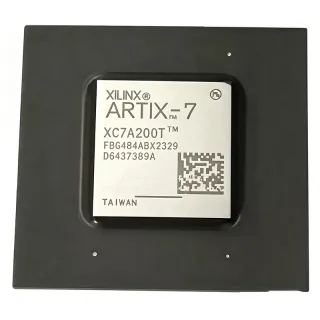
EP2C35F484C8 - Cyclone II FPGA 33K LEs 484-FBGA | Intel / Altera
MPN: EP2C35F484C8 ✗ 停產EP2C35F484C8 概覽
Background: A Field Programmable Gate Array (FPGA) is a semiconductor IC built around an array of configurable logic blocks (CLBs / LEs) connected by programmable interconnect. FPGAs sit in the programmable logic hierarchy alongside CPLDs, with FPGAs offering higher logic density and richer DSP/memory resources. The Cyclone II family positioned Intel/Altera in the low-cost FPGA segment, providing ASIC-level integration at FPGA pricing for consumer, industrial, and wireless applications.
Key features include 35 embedded 18x18 multipliers for DSP, up to 4 PLLs per device for clock management, support for external memory interfaces including DDR/DDR2/QDRII SDRAM, and 1.2V core operation with hot-socketing support. Configuration is handled via passive serial (PS), fast passive parallel (FPP), active serial (AS), or JTAG modes, supported by industry-standard Quartus II design tools. The device is fabricated on a 90nm low-k CMOS process.
Typical applications include video surveillance and image processing pipelines, industrial motor control and factory automation controllers, low-cost wireline/wireless baseband processing, PCI/PCI-X bridge designs, and display controllers. The combination of high logic density, embedded multipliers, and broad memory interface support makes the EP2C35F484C8 particularly well-suited to mid-complexity DSP and control-plane designs.
Design consideration: Successful PCB layout requires careful attention to the 484-ball BGA fanout, power distribution (VCCINT 1.2V, VCCIO banked 1.5V/1.8V/2.5V/3.3V), and decoupling. Use a multi-layer PCB with dedicated power and ground planes; place 0.1uF and 10uF decoupling capacitors close to each power pin. The Cyclone II datasheet provides reference board layouts and signal-integrity guidelines that should be followed.
This page synthesizes distributor pricing, drop-in same-family variants, and practical FPGA design notes not aggregated in a single manufacturer document.
直接替換替代品,適用於 EP2C35F484C8 — 相同封裝,腳位對腳位相容。需重新設計 PCB 的不同封裝零件不列入。
此系列的變體
與下列產品可直接替換的同系列型號: EP2C35F484C8 (相同外形與佔位) — 差異在於 Operating Temperature, Package, Process Technology, Speed Grade, Configuration Modes.
EP2C35F484C8N
✅ 直接替換聯絡詢價
查看資料表 →EP2C35F484C7N
✅ 直接替換聯絡詢價
查看資料表 →EP2C35F484C7
✅ 直接替換聯絡詢價
查看資料表 →EP2C35F484C6N
✅ 直接替換聯絡詢價
查看資料表 →EP2C35F484C6
✅ 直接替換聯絡詢價
查看資料表 →EP2C35F484C8 最大額定值與電氣特性
| Series | Cyclone II |
| Logic Elements (LEs) | 33,216 |
| Total RAM Bits | 483,840 |
| Number of I/O Pins | 322 |
| Number of Logic Blocks / Cells | 2,100 |
| Number of Multipliers (18x18) | 35 |
| Number of PLLs | 4 |
| Supply Voltage (VCCINT) | 1.2 V |
| Logic Family | CMOS |
| Package Type | FBGA-484 |
| Pins | 484 |
| 安裝類型 | Surface Mount |
| 工作溫度 | 0C to +85C (Commercial) |
| Speed Grade | 8 |
| Process Technology | 90 nm CMOS |
| RoHS 狀態 | Compliant |
| Configuration Mode | Passive Serial / Fast Passive Parallel / Active Serial / JTAG |
EP2C35F484C8 fbga-484 腳位配置指南
EP2C35F484C8(fbga-484 封裝)的腳位配置。 此數位 IC 包含 GPIO、通訊介面(UART、SPI、I2C)與電源腳位。替代腳位功能與配置選項請參閱製造商資料表。對嵌入式系統設計與 PCB 佈局至關重要。

無詳細腳位定義資料: EP2C35F484C8.
請參閱 資料表 以查看完整腳位配置。
典型應用
EP2C35F484C8 適用於 6 應用s: Video Surveillance and Image Processing, Industrial Motor Control, Communications Line Cards and Protocol Bridging, PCI/PCI-X Bridge Designs, Display Controllers and LCD Interfaces, Education, Prototyping and FPGA Learning Kits.
Video Surveillance and Image Processing
The EP2C35F484C8 is well suited to mid-complexity video surveillance and image-processing pipelines because it combines 33,216 LEs of fabric with 35 embedded 18x18 multipliers and 483,840 bits of block RAM. Designers typically implement Sobel-edge detection, motion estimation, or H.264 baseline encode at D1 resolution using the DSP blocks for FIR filtering and the M4K/M512 memory blocks for line buffering. Compared to a discrete DSP-plus-ASIC solution, the FPGA offers a single-chip BOM and field-upgradable firmware, which is critical when surveillance standards evolve.
推薦
Industrial Motor Control
The EP2C35F484C8 is widely deployed in industrial motor control and factory-automation controllers where deterministic real-time response is required. The 322 user I/Os allow direct interfacing to multiple encoder channels, Hall-effect sensors, and PWM gate drivers for three-phase inverters, while the 35 hardware multipliers accelerate field-oriented control (FOC) and space-vector PWM (SVPWM) loops. The 4 PLLs provide the precise clock synthesis needed for resolver excitation and high-speed ADC sampling. Designers targeting IEC 61131-3 industrial PLCs leverage the FPGA as a co-processor to the main MCU.
推薦
Communications Line Cards and Protocol Bridging
Wireline communications line cards and protocol-bridging designs use the EP2C35F484C8 for packet classification, traffic shaping, and bridging between legacy TDM/E1 and modern Ethernet backplanes. The device's 322 user I/Os support multiple SGMII/GMII interfaces plus glue logic to a network processor, while the 483 Kbits of block RAM provide ample on-chip buffer space for queue management. The integrated 4 PLLs allow independent clock domains for TDM and Ethernet sides, simplifying clock-tree synthesis in hybrid TDM/IP equipment.
推薦
PCI/PCI-X Bridge Designs
The EP2C35F484C8 is frequently used as a PCI-to-local-bus bridge in industrial PCs and embedded SBCs, replacing legacy ASIC bridge chips that have become EOL. With 33,216 LEs, the FPGA can implement the full PCI 32-bit/33MHz target or initiator state machine, scatter-gather DMA, and additional glue logic for legacy ISA or local-bus peripherals. The 322 user I/Os allow expansion to multiple downstream buses, and the JTAG interface simplifies boundary-scan compliance testing during board bring-up.
推薦
Display Controllers and LCD Interfaces
The EP2C35F484C8 is used in industrial display controllers, panel-meter HMIs, and kiosk LCD interfaces where flexible timing generation and on-the-fly color-space conversion are required. The 322 user I/Os support parallel RGB/TTL panels up to XGA resolution while leaving pins for capacitive-touch controllers and backlight PWM. Designers implement timing controllers (TCON), dithering, and overdrive compensation in fabric, accelerating time-to-market compared to fixed-function LCD controller ASICs.
推薦
Education, Prototyping and FPGA Learning Kits
The EP2C35F484C8 appears in many university and hobbyist FPGA development boards because it offers generous logic density (33,216 LEs) at an accessible price point, supporting projects that would otherwise outgrow smaller Cyclone II variants. The FBGA-484 package is well supported on standard 4-layer dev boards with 1.0mm BGA pitch. Combined with the Quartus II Web Edition toolchain, learners can implement CPUs, signal-processing pipelines, and custom peripherals. Although the device is NRND, surplus inventory remains broadly available for educational use as of 2026-09-08.
推薦
推薦產品摘要
工程參考資料,適用於 EP2C35F484C8 — 比較、設計指引及合規資訊。
選型指南
與替代品比較
| 參數 | 本產品 | EP2C35F484C8N | EP2C35F484C7N | EP2C35F484C7 | EP2C35F484C6N | EP2C35F484C6 |
|---|---|---|---|---|---|---|
| Package | FBGA-484 (1.0mm pitch) | FBGA-484 (1.0mm pitch) - same | FBGA-484 (1.0mm pitch) - same | FBGA-484 (1.0mm pitch) - same | FBGA-484 (1.0mm pitch) - same | FBGA-484 (1.0mm pitch) - same |
| Brand | Altera (Intel) | Altera (Intel) | Altera (Intel) | Altera (Intel) | Altera (Intel) | Altera (Intel) |
| Logic Elements | 33,216 LEs | 33,216 LEs | 33,216 LEs | 33,216 LEs | 33,216 LEs | 33,216 LEs |
| Speed Grade | 8 | 8 | 7 | 7 | 6 | 6 |
| Embedded RAM | 483,840 bits | 483,840 bits | 483,840 bits | 483,840 bits | 483,840 bits | 483,840 bits |
| Multipliers (18x18) | 35 | 35 | 35 | 35 | 35 | 35 |
| User I/O Pins | 322 | 322 | 322 | 322 | 322 | 322 |
| RoHS / Lead-Free | Standard (non-N) | Lead-free / RoHS | Lead-free / RoHS | Standard (non-N) | Lead-free / RoHS | Standard (non-N) |
| Lifecycle Status | NRND | NRND | NRND | NRND | NRND | NRND |
主要差異化特點
- Higher speed grade than C6/C7 same-family variants (對比EP2C35F484C6N)
- Lead-free bump finish versus non-N variant (對比EP2C35F484C8N)
- Mid-density LE count versus lower-density siblings (對比EP2C20F484C8)
設計說明
Estimated: The 484-ball FBGA with 1.0mm pitch requires a 4- or 6-layer PCB with 0.4-0.5mm laser-drilled microvias to fan out the inner-row balls. Use a 0.2032mm (8 mil) trace-and-space design rule with a 0.4mm via pad for outer-row escape, and follow the Cyclone II Device Handbook reference stackup. Power planes must be continuous beneath the BGA; split planes for VCCINT 1.2V and VCCIO banks to avoid return-path discontinuities. Verify signal-integrity simulation on DDR2 and LVDS routes before fab.
Power the EP2C35F484C8 from a 1.2V regulator with at least 1.5A headroom plus separate 1.2V analog PLL supplies. Place 0.1uF X7R 0402/0201 decoupling capacitors on every VCCINT pin and 10uF bulk capacitors per quadrant; VCCIO banks each need their own 0.1uF decoupling network sized to the switching I/O count. Sequence the VCCINT and VCCIO rails according to the Cyclone II handbook to avoid hot-socketing latchup.
Three pitfalls to avoid with this part: (1) using a non-N suffix in a RoHS-restricted application or vice-versa (bump finish affects solder profile); (2) choosing speed grade 8 when speed grade 6 or 7 would close timing, doubling unit cost unnecessarily; (3) placing configuration flash too far from the FPGA, causing AS-mode boot failures. Estimated: for a typical 33-LE design with 60% utilization at 200MHz Fmax, a C6 speed grade is usually sufficient.
合規資訊
Non-N suffix variant uses leaded bump finish (non-RoHS). For RoHS applications use EP2C35F484C8N. AEC-Q100 not applicable - this is a commercial-grade FPGA; industrial-grade -I variants exist separately (EP2C35F484I8).