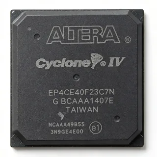
EP2S15F484C5N - Stratix II FPGA, 15K LEs, 484-FBGA | Intel
MPN: EP2S15F484C5N ✗ 停產EP2S15F484C5N 概覽
An FPGA (Field-Programmable Gate Array) is a type of programmable logic device (PLD) that allows designers to implement custom digital circuits through configuration memory rather than fixed mask lithography. FPGAs sit within the broader hierarchy of semiconductors: programmable logic -> PLD -> FPGA -> high-density FPGA. Stratix II devices occupy the high-performance tier of this hierarchy, offering dedicated DSP blocks, embedded transceivers on selected variants, and TriMatrix embedded memory that accelerates DSP, video, and packet-processing pipelines.
Key features of the EP2S15F484C5N include 15,600 LEs, 419 Kbits of embedded RAM, dedicated DSP blocks for fixed- and floating-point arithmetic, support for external memory interfaces including DDR/DDR2 SDRAM and QDR II SRAM, and up to 342 user I/O pins. The -C5 speed grade designates a balanced performance/power operating point, while the industrial temperature range supports deployment in demanding environments. Internal configuration is achieved through active serial (AS), passive serial (PS), or JTAG interfaces.
Architecturally, the Stratix II family introduced an adaptive logic module (ALM) structure that improved logic utilization versus prior architectures, paired with high-speed Row/Column interconnect. The device integrates PLLs for clock management, supports source-synchronous interfaces up to 1 Gbps on selected pins, and includes hardware multipliers optimized for DSP pipelines. The 484-FBGA package exposes enough I/O to drive multiple DDR2 channels in parallel.
Typical applications for the EP2S15F484C5N include telecom line cards, baseband signal processing, video format conversion, military and aerospace signal processing, ASIC prototyping, and high-performance DSP coprocessing. The device is well suited as a hardware accelerator for compute-intensive algorithms or as a prototyping vehicle prior to ASIC tape-out.
When designing with this device, allocate sufficient decoupling across the multi-rail supply pins (VCCINT, VCCIO, VCCA, VCCD_PLL), follow the Stratix II pin connection guidelines to tie unused pins to defined logic levels, and validate timing closure using the Quartus II design suite. PCB layout should target matched impedance for high-speed transceiver and DDR2/QSPI routes.
This page synthesizes distributor pricing, drop-in package-compatible Stratix II alternatives, comparison data, and practical design notes not collated in the manufacturer datasheet alone.
直接替換替代品,適用於 EP2S15F484C5N — 相同封裝,腳位對腳位相容。需重新設計 PCB 的不同封裝零件不列入。
此系列的變體
與下列產品可直接替換的同系列型號: EP2S15F484C5N (相同外形與佔位) — 差異在於 Speed Grade, Package, RoHS Status, Adaptive Logic Modules (ALMs), Configuration Method.
EP2S15F484C5
✅ 直接替換聯絡詢價
查看資料表 →EP2S15F484C4N
✅ 直接替換聯絡詢價
查看資料表 →EP2S15F484C3N
✅ 直接替換聯絡詢價
查看資料表 →EP2S15F484C3
✅ 直接替換聯絡詢價
查看資料表 →EP2S15F484C4
✅ 直接替換✗ 缺貨
$205 / 單位
查看資料表 →EP2S15F484C5N 最大額定值與電氣特性
| Family | Stratix II |
| Logic Elements (LEs) | 15,600 |
| Embedded RAM | 419 Kbits |
| Maximum User I/O | 342 |
| Process Technology | 90 nm |
| 封裝 | 484-ball FineLine BGA (FBGA) |
| Speed Grade | C5 |
| Configuration Modes | AS, PS, JTAG |
| External Memory Support | DDR/DDR2 SDRAM, QDR II SRAM |
| 安裝類型 | Surface Mount |
EP2S15F484C5N 484-ball fineline bga (fbga) 腳位配置指南
EP2S15F484C5N(484-ball fineline bga (fbga) 封裝)的腳位配置。 此數位 IC 包含 GPIO、通訊介面(UART、SPI、I2C)與電源腳位。替代腳位功能與配置選項請參閱製造商資料表。對嵌入式系統設計與 PCB 佈局至關重要。

無詳細腳位定義資料: EP2S15F484C5N.
請參閱 資料表 以查看完整腳位配置。
典型應用
EP2S15F484C5N 適用於 6 應用s: Telecom Line Card Processing, Baseband Signal Processing, Video Format Conversion and Processing, ASIC Prototyping, High-Performance DSP Coprocessor, Military and Aerospace Signal Processing.
Telecom Line Card Processing
The EP2S15F484C5N fits telecom line-card designs that demand mid-range logic density plus dedicated DSP blocks for packet processing. The 15,600 LE budget, combined with 342 user I/O from the 484-FBGA package, exposes enough pins to drive multi-channel SERDES, TDM buses, and framer interfaces concurrently. Its embedded TriMatrix RAM (419 Kbits) holds lookup tables and packet buffers at line rate without external memory contention. Compared with discrete DSP+ASIC partitioning, a single Stratix II consolidates the datapath, shortens time-to-market, and supports field reconfiguration as protocols evolve. Design tip: pair the FPGA with an external TCAM and DDR2 SDRAM for full L2/L3 forwarding.
推薦
Baseband Signal Processing
The EP2S15F484C5N serves baseband DSP pipelines where multiple fixed-point multipliers operate in parallel. Stratix II DSP blocks deliver dedicated hardware multipliers with accumulator support, freeing LEs for control logic. The C5 speed grade provides the highest Fmax in the EP2S15 density, enabling longer FFT/IFFT stages per pipeline stage and reducing the number of time-multiplexed iterations. The 484-FBGA package supports board-level integration with RF front-end ADCs and DACs at matched impedance. Compared with software-defined radio on a microcontroller, this FPGA offloads compute-intensive kernels with deterministic latency, which is essential for LTE/WiMAX baseband.
推薦
Video Format Conversion and Processing
The EP2S15F484C5N handles real-time video format conversion (e.g., SD/HD upconversion, deinterlacing, scaling) by exploiting parallel pixel-pipeline architectures. The 342 user I/O pins from the 484-FBGA package connect directly to digital video interfaces such as BT.656, BT.1120, and HDMI link layers, while embedded RAM buffers full video frames at common resolutions. The C5 speed bin enables higher pixel clock rates needed for 1080p60 throughput. Compared with a dedicated video ASIC, the FPGA supports evolving standards and custom deinterlacing algorithms with hardware-software co-design in C-to-hardware flows.
推薦
ASIC Prototyping
The EP2S15F484C5N provides a credible prototyping vehicle for ASIC designs targeting the same logic-density range. Designers map synthesizable ASIC RTL to the Stratix II ALM structure, validate timing with the Quartus II toolchain, and exercise real-world I/O at near-ASIC performance. The 484-FBGA package exposes enough user I/O to replicate most ASIC pad-ring scenarios, and configuration bitstreams can be regenerated quickly for design iterations. Compared with hardware emulators, individual FPGAs deliver faster compile cycles at lower cost per design, ideal for sub-million-gate ASIC pre-silicon validation.
推薦
High-Performance DSP Coprocessor
The EP2S15F484C5N functions as a hardware DSP accelerator sitting alongside a host processor over PCI, PCIe, or a parallel host bus. Stratix II DSP blocks accelerate FIR filters, FFTs, and matrix multiplications at clock rates unattainable in software, freeing the host for control tasks. The 484-FBGA package exposes multi-bank DDR2 interfaces for high-bandwidth data streaming. Compared with a software DSP library on a general-purpose CPU, the FPGA delivers 10x-100x speedups on inner-loop kernels while keeping the host free for I/O. Useful in radar, sonar, and medical imaging accelerators.
推薦
Military and Aerospace Signal Processing
The EP2S15F484C5N is well suited to military and aerospace signal-processing platforms that demand ruggedized operation. Its industrial temperature grade supports harsh-environment deployments, while 15,600 LEs accommodate channelization, beamforming, and cryptography pipelines. The 484-FBGA package, though not the largest in the family, provides ample I/O for multi-channel ADC/DAC interfacing. Compared with ASIC equivalents, the FPGA supports in-field firmware updates for evolving threat libraries, a major advantage in long-lifecycle programs. Designers must validate upscreen and hermeticity per program requirements.
推薦
工程參考資料,適用於 EP2S15F484C5N — 比較、設計指引及合規資訊。
選型指南
與替代品比較
| 參數 | 本產品 | EP2S15F484C5 | EP2S15F484C4N | EP2S15F484C3N | EP2S15F484C3 | EP2S15F484C4 |
|---|---|---|---|---|---|---|
| Package | 484-FBGA | 484-FBGA - same | 484-FBGA - same | 484-FBGA - same | 484-FBGA - same | 484-FBGA - same |
| Brand | Intel (formerly Altera) | Intel | Intel | Intel | Intel | Intel |
| Logic Elements (LEs) | 15,600 | 15,600 | 15,600 | 15,600 | 15,600 | 15,600 |
| Speed Grade | C5 | C5 | C4 (slower) | C3 (slowest) | C3 (slowest) | C4 (slower) |
| Temperature Grade | Industrial (N suffix) | Commercial (no N suffix) | Industrial | Industrial | Commercial | Commercial |
| Embedded RAM | 419 Kbits | 419 Kbits | 419 Kbits | 419 Kbits | 419 Kbits | 419 Kbits |
| Maximum User I/O | 342 | 342 | 342 | 342 | 342 | 342 |
| Lifecycle Status | Obsolete | Obsolete | Obsolete | Obsolete | Obsolete | Obsolete |
主要差異化特點
- Fastest speed grade in EP2S15 density tier (對比EP2S15F484C3N)
- Industrial temperature grade with full Stratix II feature set (對比EP2S15F484C5)
- Identical die to all other 484-FBGA EP2S15 variants (對比All listed drop-in alternatives)
設計說明
The 484-FBGA package requires 4-6 layer PCB with controlled-impedance routing and via-in-pad or microvia technology for reliable assembly. Decoupling capacitors must be placed within 100 mils of each power ball, separating VCCINT, VCCIO, VCCA, and VCCD_PLL rails. Per the Stratix II device handbook pin connection guidelines, unused I/O pins should be tied to defined logic levels rather than left floating to avoid leakage.
Stratix II FPGAs at full utilization with C5 speed grade can dissipate significant power, especially with high toggle rates on DDR2 interfaces. Estimated: at 60% utilization and 200 MHz operation, junction temperature can exceed 90C without airflow or thermal vias to inner copper planes. Provide a thermal pad or heat spreader connected through thermal vias to inner ground planes; design for theta_JA of approximately 15 C/W with 1 oz copper pours to inner planes.
Common pitfalls include failing to assign all configuration pins (nCONFIG, nSTATUS, CONF_DONE, MSEL[3:0]) to valid logic levels, mixing VCCIO banks at incompatible voltages on shared banks, and exceeding the Stratix II absolute maximum ratings on PLL supply noise. Always generate configuration bitstreams using the Quartus II tool version matching the device handbook revision used for design capture, and verify pin assignments with the pin-planner before board fabrication.
合規資訊
Compliance data not present in the verified web search results; refer to the manufacturer datasheet for RoHS, REACH, lead-free, and halogen-free certifications specific to this lot.