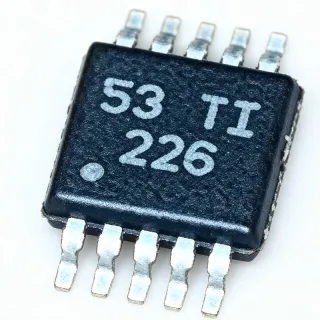
INA2181A1QDGSRQ1 - 26V Dual Ch Current Sense Amp, A1 Gain | TI
MPN: INA2181A1QDGSRQ1 ✓ 啟用中INA2181A1QDGSRQ1 概覽
A current-sense amplifier is a specialized difference amplifier that measures the small voltage drop across a shunt resistor and converts it to a ground-referenced output signal. It sits within the broader signal-chain hierarchy: current-shunt monitor -> current-sense amplifier -> instrumentation amplifier -> analog front end -> power-management system. Current monitors like the INAx181 family are essential for battery management, fault detection, and closed-loop current control.
Key features include the dual-channel integration, which lets one device monitor two shunts (for example high-side and low-side rails) and saves board area versus two single-channel parts. The wide -0.2 V to 26 V common-mode range allows placement on high-side or low-side rails independent of the 1.7 V to 5.5 V supply. Rail-to-rail output swing and a bidirectional architecture support charge and discharge monitoring around a programmable reference. The automotive Q1 rating extends operating temperature to 125C ambient.
Architecturally, the INA2181-Q1 uses a precision, cost-optimized topology derived from the single-channel INA181-Q1. Gain is factory-set to 20 V/V in the A1 grade, with offset, gain error, and bandwidth trimmed to deliver predictable accuracy at low system cost. The 350 kHz bandwidth permits monitoring of switching currents in moderate-frequency power converters.
Typical applications include automotive 12 V and 24 V battery supervision, automotive body and powertrain modules, telecom and industrial power supplies, and motor-drive DC bus monitoring. The voltage-output interface connects directly to ADC inputs on MCUs such as the TMS320F28032.
Design consideration: budget for input common-mode transients above 26 V during automotive load-dump events; TI specifies the device tolerates brief common-mode excursions, but sustained overvoltage requires external series resistance or clamp protection.
This page synthesizes distributor pricing, same-family drop-in gain variants, and practical design notes not found in the manufacturer datasheet.
直接替換替代品,適用於 INA2181A1QDGSRQ1 — 相同封裝,腳位對腳位相容。需重新設計 PCB 的不同封裝零件不列入。
此系列的變體
與下列產品可直接替換的同系列型號: INA2181A1QDGSRQ1 (相同外形與佔位) — 差異在於 Output Type, Package, Qualification, Bandwidth, Common-Mode Voltage Range.
INA2181A2QDGSRQ1
✅ 直接替換聯絡詢價
查看資料表 →INA2181A3QDGSRQ1
✅ 直接替換聯絡詢價
查看資料表 →INA2181A4QDGSRQ1
✅ 直接替換聯絡詢價
查看資料表 →INA2181A1DGS
✅ 直接替換📋 參考替代品(不在目錄中)
INA2181A1QDGSTQ1
✅ 直接替換 ⚠️ 規格未經驗證📋 參考替代品(不在目錄中)
INA2181A1QDGSRQ1 最大額定值與電氣特性
| 通道數 | 2 (dual-channel) |
| Gain (A1 option) | 20 V/V |
| Bandwidth | 350 kHz (typ) |
| Common-Mode Voltage Range | -0.2 V to 26 V (independent of supply) |
| Supply Voltage Range | 1.7 V to 5.5 V |
| 輸出類型 | Voltage output, rail-to-rail |
| Measurement Topology | Bidirectional, low-side and high-side |
| 工作溫度範圍 | -40C to +125C |
| 封裝 | 10-pin VSSOP (DGS) |
| 安裝類型 | Surface Mount |
| Qualification | AEC-Q100 qualified |
| RoHS 狀態 | Compliant |
| Family | INAx181-Q1 (INA181-Q1, INA2181-Q1, INA4181-Q1) |
| Reference Pins | REF1 and REF2 for bidirectional offset |
INA2181A1QDGSRQ1 10-pin vssop (dgs) 腳位配置指南
INA2181A1QDGSRQ1(10-pin vssop (dgs) 封裝)的腳位配置。 腳位編號、功能與連接圖定義於製造商資料手冊中。請參閱該手冊以取得確切的封裝尺寸與焊接指引。

無詳細腳位定義資料: INA2181A1QDGSRQ1.
請參閱 資料表 以查看完整腳位配置。
典型應用
INA2181A1QDGSRQ1 適用於 6 應用s: Automotive 12V Battery Monitoring, Automotive Body and Powertrain Modules, 24V Industrial and Telecom Power Supplies, Motor Drive DC Bus and Phase Current Supervision, Battery-Management Systems (BMS), USB and Port Power Monitoring.
Automotive 12V Battery Monitoring
The INA2181A1QDGSRQ1 fits automotive battery supervision because its -0.2 V to 26 V common-mode range covers 12 V battery rails through cold-crank dips and normal charge conditions, while AEC-Q100 qualification and -40C to +125C operation satisfy body-electronics environmental requirements. Each of the two channels can monitor the charge path and the discharge path of the battery with separate shunts, using REF1/REF2 biasing to represent both current polarities. Placed high-side between the battery positive terminal and the load fuse with a 1 to 5 mOhm shunt, the 20 V/V A1 gain delivers an ADC-ready voltage output directly to a 3.3 V MCU input. The 350 kHz bandwidth is ample for millisecond-scale load transients; adding a simple RC anti-alias filter ahead of the ADC removes wideband noise from the rail.
推薦
Automotive Body and Powertrain Modules
Body-control, lighting, and powertrain modules require cost-optimized current monitoring of multiple loads, and the INA2181A1QDGSRQ1 addresses this with two independent channels in one 10-pin VSSOP package, halving solution footprint versus two single-channel amplifiers. The 26 V common-mode rating tolerates 12 V rail fluctuations including load-transient conditions typical in body electronics, while the Q1 qualification supports PPAP submission for automotive production. With the A1 gain of 20 V/V, engineers can use larger, lower-cost shunt resistors (5 to 10 mOhm) with relaxed PCB copper requirements, and the rail-to-rail output preserves measurement range down to millivolt shunt drops. The voltage-output architecture interfaces without additional signal conditioning to standard automotive MCU ADC inputs, keeping the bill of materials minimal for cost-sensitive ECUs.
推薦
24V Industrial and Telecom Power Supplies
Industrial 24 V backplanes and telecom rectifier boards benefit from the INA2181A1QDGSRQ1 because its 26 V maximum common-mode rating sits just above the 24 V nominal rail, allowing direct high-side connection without level shifting. The dual channels let one device monitor both the input feed and the output rail of a DC-DC module, or two paralleled rectifier branches for load balancing. The 1.7 V to 5.5 V supply range means the amplifier can run from the controller's 3.3 V or 5 V logic supply even while sensing the 24 V bus, simplifying power distribution on the board. With 350 kHz bandwidth, the device captures inrush and switching ripple envelope at moderate fidelity, and the A1 20 V/V gain keeps output swing within ADC range for the multi-amp currents typical of telecom shelves.
推薦
Motor Drive DC Bus and Phase Current Supervision
In low-voltage motor drives, the INA2181A1QDGSRQ1 supervises the DC bus current on the high side of the shunt, providing overcurrent detection feedback to MCUs such as the C2000 family. The 350 kHz bandwidth captures the switching-frequency current envelope for drives switching at 20 to 50 kHz with reasonable fidelity, and the bidirectional architecture with REF biasing represents both motoring and regenerative current polarity. Because the common-mode range extends to 26 V independent of the amplifier supply, a single 3.3 V-powered device monitors a 12 V or 24 V drive bus directly. The A1 gain suits the larger shunts commonly used for thermal robustness in industrial drives; pairing with a filtered output RC network prevents aliasing of switching ripple in the ADC sampling path.
推薦
Battery-Management Systems (BMS)
Portable and backup battery systems use the INA2181A1QDGSRQ1 for coulomb-counting and protection current measurement. The bidirectional topology, offset by the REF pins, naturally captures charge and discharge current through a single low-side shunt per channel, enabling state-of-charge integration in the host MCU. The rail-to-rail output maximizes ADC dynamic range at low shunt drops, improving resolution at light loads, while the low-cost dual-channel integration monitors both the battery pack and the system load rail simultaneously. Because common-mode sensing extends to -0.2 V, inductive voltage reversals during load steps do not saturate the input stage. The 1.7 V minimum supply supports single-cell Li-ion powered designs after a simple regulator, and the small VSSOP-10 footprint suits space-constrained pack electronics.
推薦
USB and Port Power Monitoring
Smart USB-C and hot-swap port designs use the INA2181A1QDGSRQ1 to measure delivery current on the VBUS high side. The 26 V common-mode ceiling covers USB PD 100 W (20 V) rails with margin, and the 1.7 V to 5.5 V supply runs from the port controller's low-voltage rail. The A1 20 V/V gain with a 5 to 10 mOhm shunt produces a well-conditioned signal for port-current reporting and overload detection thresholds in firmware, while the fast 350 kHz response flags short-circuit transients within microseconds-scale windows. Two channels allow monitoring both a source port and a sink port from one device, useful in dual-role-power hubs. The rail-to-rail output maps cleanly onto 3.3 V ADC inputs, and REF grounding provides unidirectional measurement from zero current.
推薦
推薦產品摘要
工程參考資料,適用於 INA2181A1QDGSRQ1 — 比較、設計指引及合規資訊。
選型指南
與替代品比較
| 參數 | 本產品 | INA2181A2QDGSRQ1 | INA2181A3QDGSRQ1 | INA2181A4QDGSRQ1 | INA2181A1DGS |
|---|---|---|---|---|---|
| Package | 10-pin VSSOP (DGS) | 10-pin VSSOP (DGS) - same | 10-pin VSSOP (DGS) - same | 10-pin VSSOP (DGS) - same | 10-pin VSSOP (DGS) - same |
| Brand | Texas Instruments | Texas Instruments | Texas Instruments | Texas Instruments | Texas Instruments |
| Gain | 20 V/V (A1) | 50 V/V (A2) | 100 V/V (A3) | 200 V/V (A4) | 20 V/V (A1) |
| Channels | 2 (dual) | 2 (dual) | 2 (dual) | 2 (dual) | 2 (dual) |
| Common-Mode Range | -0.2 V to 26 V | -0.2 V to 26 V | -0.2 V to 26 V | -0.2 V to 26 V | -0.2 V to 26 V |
| Bandwidth | 350 kHz | 350 kHz | 350 kHz | 350 kHz | 350 kHz |
| AEC-Q100 Qualification | Yes (Q1) | Yes (Q1) | Yes (Q1) | Yes (Q1) | No (commercial grade) |
| Temperature Range | -40C to +125C | -40C to +125C | -40C to +125C | -40C to +125C | -40C to +125C |
| Typical Application Shunt | 5-10 mOhm (larger shunts) | 2-5 mOhm | 1-2 mOhm | 0.5-1 mOhm (lowest loss) | 5-10 mOhm |
主要差異化特點
- Lowest gain grade enables largest shunts and widest overload headroom (對比INA2181A4QDGSRQ1)
- Dual-channel integration halves board area versus two single-channel parts (對比INA181A1 (single channel))
- AEC-Q100 automotive flow for the same silicon (對比INA2181A1DGS)
- Trade-off: 350 kHz bandwidth is modest for fast switching (對比Higher-bandwidth current-sense amplifiers (e.g., INA240-class))
設計說明
Use Kelvin connections to the shunt resistor: route IN+ and IN- traces directly to the shunt pads rather than sharing the current-carrying copper. Any milliohm of trace resistance adds directly to the measured shunt and scales as a gain error. Keep the two input traces as a tightly coupled differential pair, and place the INA2181A1QDGSRQ1 within a few millimeters of the shunt. Ground the REF1/REF2 pins to a quiet analog ground with a local 0.1 uF bypass; noise on REF appears 1:1 at the output.
Power the amplifier from the cleanest available logic rail (1.7 V to 5.5 V) with a 0.1 uF ceramic capacitor placed within 2 mm of the supply pin. Because common-mode sensing is independent of supply, the amplifier supply choice affects only output swing and ADC interface compatibility: a 3.3 V supply limits full-scale output near 3.3 V, so size the shunt and gain so maximum current maps to about 90% of the ADC range. Estimated: with 20 V/V gain and 3.3 V logic, a 10 mOhm shunt full-scales near 15 A.
Do not exceed the 26 V common-mode rating: automotive load-dump transients on 12 V rails can far exceed this briefly, so verify the module's clamping strategy (TVS diodes upstream) before connecting the sense inputs. Also remember that gain grades (A1 vs A2/A3/A4) share the same footprint - if a purchasing substitution swaps gain grades, firmware current scaling becomes wrong by 2.5x to 10x. Encode the expected gain in firmware validation or lock the BOM to the A1 grade to prevent this silent miscalibration.
The 350 kHz bandwidth passes switching ripple from PWM loads; add an RC low-pass filter between the output and the MCU ADC pin (for example 1 kOhm and 10 nF, estimated 16 kHz cutoff) to average switching currents and prevent aliasing. If cycle-by-cycle peak detection is needed instead, reduce the filter and sample synchronously with the PWM carrier. Keep OUT traces away from gate-driver and clock routing to avoid coupled spikes on this relatively high-impedance analog output.
合規資訊
AEC-Q100 qualified per TI product page and datasheet (Rev. F). RoHS and lead-free status per standard TI automotive flow; REACH and halogen-free status not stated in the provided data.