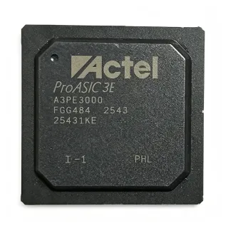
LFE2-35E-5F484C - 32K LUT ECP2 FPGA | Lattice Semiconductor
MPN: LFE2-35E-5F484C ✓ 啟用中LFE2-35E-5F484C 概覽
An FPGA is a reconfigurable digital semiconductor that combines programmable logic blocks with programmable interconnect resources. At the system level, it belongs to the programmable-logic hierarchy: FPGA, programmable-logic device, digital integrated circuit, and semiconductor. Unlike a fixed-function microcontroller or application processor, an FPGA implements parallel hardware logic that can be rewritten for different protocols, data paths, or control functions after manufacture.
The ECP2 family provides 32,000 LUTs, 331 I/O, and advanced DSP blocks in the specified device. The 1.2 V core operating voltage supports modern low-voltage digital designs, while the 484-FBGA package offers a dense route for implementing many board-level interfaces in a compact component. The -5 ordering suffix identifies the selected Lattice speed and temperature grade, and the trailing C identifies the commercial package configuration.
At an architectural level, the FPGA fabric can implement parallel datapaths, control logic, protocol bridges, and fixed-point or filtered DSP functions. The embedded DSP blocks accelerate suitable arithmetic workloads while programmable interconnect routes signals between LUTs, registers, memories, block RAM, DSP elements, and I/O. Designers must still map clocks, resets, buses, and interfaces in the development tool and verify timing after each implementation.
Typical uses include industrial control, data acquisition, communications infrastructure, embedded vision, instrumentation, and general-purpose digital signal processing. Its combination of 331 I/O and programmable logic is especially useful when a design needs many parallel external connections, custom serial protocols, or multiple independent processing pipelines rather than a single sequential processor core.
Board design should follow the manufacturer pinout and recommended decoupling guidance for the 484-FBGA package. Confirm that every power, ground, configuration, clock, and high-speed signal connection matches the selected device variant, and route configuration pins so the FPGA enters a valid operating state during power-up, reset, and reprogramming events.
This product overview combines the device's verified architecture and ordering information with family-level comparison data and practical implementation guidance. It helps engineers evaluate the LFE2-35E-5F484C for high-density programmable-logic, DSP, control, and I/O-intensive designs before completing device-specific schematic and timing review.
直接替換替代品,適用於 LFE2-35E-5F484C — 相同封裝,腳位對腳位相容。需重新設計 PCB 的不同封裝零件不列入。
LFE2-35E-5FN484C
✅ 直接替換📋 參考替代品(不在目錄中)
LFE2-35SE-6F484C
✅ 直接替換📋 參考替代品(不在目錄中)
LFE2-35SE-5F484C
✅ 直接替換📋 參考替代品(不在目錄中)
LFE2-35E-6FN484C
✅ 直接替換📋 參考替代品(不在目錄中)
LFE2M35E-5FN484C
✅ 直接替換📋 參考替代品(不在目錄中)
LFE2-35E-5F484C 最大額定值與電氣特性
| Device Type | ECP2 Field-Programmable Gate Array (FPGA) |
| Look-Up Tables | 32,000 LUTs |
| I/O Sites | 331 I/O |
| Core Supply Voltage | 1.2 V |
| Speed Grade | -5 |
| 封裝 | 484-FBGA |
| DSP Capability | Advanced DSP blocks |
| Programmable Logic | 32,000 LUTs |
| Device Family | LatticeECP2 |
| 安裝類型 | Surface Mount |
| Ball Count | 484 balls |
LFE2-35E-5F484C 484-fbga 腳位配置指南
LFE2-35E-5F484C(484-fbga 封裝)的腳位配置。 此數位 IC 包含 GPIO、通訊介面(UART、SPI、I2C)與電源腳位。替代腳位功能與配置選項請參閱製造商資料表。對嵌入式系統設計與 PCB 佈局至關重要。

無詳細腳位定義資料: LFE2-35E-5F484C.
請參閱 資料表 以查看完整腳位配置。
典型應用
LFE2-35E-5F484C 適用於 6 應用s: Industrial Control Systems, Data Acquisition and Signal Conditioning, Communications Infrastructure, Embedded Vision and Imaging, Test and Measurement Instrumentation, Programmable Interface Consolidation.
Industrial Control Systems
The LFE2-35E-5F484C is well suited to consolidating parallel machine-control logic because it provides 32,000 LUTs and 331 I/O in a single 484-FBGA device. Engineers can implement state machines, interlocks, pulse timing, sensor conditioning logic, and actuator sequencing in parallel rather than dividing the design among multiple fixed-function controllers. Its advanced DSP blocks can also accelerate selected filtering or motion-related arithmetic. The 1.2 V core supply supports integration with modern digital logic, while the large I/O count allows numerous field-bus, encoder, and discrete I/O connections. Before schematic release, verify the selected device's I/O voltage standards, configuration startup behavior, and timing closure across the industrial operating environment.
推薦
Data Acquisition and Signal Conditioning
The LFE2-35E-5F484C can serve as the digital control layer for multi-channel measurement systems, combining 32,000 LUTs with 331 I/O for sensor gating, digital conversion control, timestamp capture, and data packing. Its advanced DSP blocks are useful for parallel filtering and fixed-point arithmetic stages, allowing the design to process multiple channels concurrently instead of relying on sequential instruction execution. The 484-FBGA package provides a dense route for connecting converters, memory, clocks, and communication logic. Designers should partition acquisition control from timing-sensitive DSP pipelines, constrain clocks appropriately, and validate conversion latency and sample alignment in the FPGA implementation.
推薦
Communications Infrastructure
The LFE2-35E-5F484C is appropriate for custom communications equipment requiring deterministic parallel logic, protocol conversion, and substantial external connectivity. Its 32,000 LUTs can support framing, header processing, queue control, and interface translation, while 331 I/O offers ample connections for parallel buses, status signals, and network-facing transceivers. The advanced DSP blocks can handle suitable symbol filtering or fixed-point signal conditioning, reducing pressure on general fabric resources. For deployment in routers, line-card equipment, or industrial communication systems, engineers should define clock domains carefully, constrain input and output timing, and verify protocol-specific error handling. Configuration pin behavior must also be checked against the system's reset and power-up sequence.
推薦
Embedded Vision and Imaging
The LFE2-35E-5F484C can implement parallel image-processing pipelines where multiple pixels or pixels-per-clock require deterministic hardware throughput. The 32,000 LUTs are suitable for control logic, feature extraction, and pipeline coordination, while the advanced DSP blocks can accelerate multiplication, accumulation, filtering, and related fixed-point operations. Its 331 I/O provides connections for image sensors, frame buffers, memory interfaces, and synchronization signals, and the 1.2 V core voltage fits contemporary digital logic. Designers should register video interfaces appropriately, constrain pixel-clock and processing paths, and analyze resource utilization after synthesis. Resource allocation must also account for frame-buffer requirements and any additional interface logic beyond the basic sensor and memory connections.
推薦
Test and Measurement Instrumentation
The LFE2-35E-5F484C is useful in programmable test and measurement equipment because it combines flexible logic density with a large number of external connections. Its 32,000 LUTs can implement sequencing engines, pattern generators, timing controls, and digital protocol analyzers, while 331 I/O allows dense connection to instruments, fixtures, and converters. The advanced DSP blocks can support selected numerical operations when a dedicated processor would add unnecessary complexity or latency. For an instrument design, engineers should partition deterministic acquisition logic from slower user-interface functions and verify jitter requirements with the selected speed grade. Clocking, isolation, calibration, and trigger synchronization require careful treatment because the 484-FBGA package presents a dense, high-speed routing challenge.
推薦
Programmable Interface Consolidation
The LFE2-35E-5F484C can consolidate several otherwise separate interface functions into one 484-FBGA device. The 32,000 LUTs provide capacity for parallel bridges, status registers, protocol state machines, and data-format converters, while 331 I/O makes the part suitable for systems with numerous narrow external signals. This is particularly useful when legacy logic, test hooks, and a new control protocol must coexist. Engineers should define the interface boundary and timing constraints before implementation, then avoid routing critical asynchronous inputs directly into long combinational paths. Configuration sequencing and board-level reset behavior should be tested across all operating modes, particularly when the FPGA controls downstream power or reset signals.
推薦
推薦產品摘要
工程參考資料,適用於 LFE2-35E-5F484C — 比較、設計指引及合規資訊。
選型指南
與替代品比較
| 參數 | 本產品 | LFE2-35E-5FN484C | LFE2-35SE-6F484C | LFE2-35SE-5F484C | LFE2-35E-6FN484C | LFE2M35E-5FN484C |
|---|---|---|---|---|---|---|
| Package | 484-FBGA | 484-FBGA | 484-FBGA | 484-FBGA | 484-FBGA | 484-FBGA |
| Brand | Lattice Semiconductor | Lattice Semiconductor | Lattice Semiconductor | Lattice Semiconductor | Lattice Semiconductor | Lattice Semiconductor |
| Core Voltage | 1.2 V | 1.2 V | 1.2 V | 1.2 V | 1.2 V | 1.2 V |
| Speed Designation | -5 | -5 | -6 | -5 | -6 | -5 |
| FPGA Family | ECP2 | ECP2 | ECP2S | ECP2S | ECP2 | ECP2M |
主要差異化特點
- Balanced logic and I/O density (對比LFE2M35E-5FN484C)
- Direct ECP2 family option (對比LFE2-35SE-5F484C)
- Consistent -5 speed designation (對比LFE2-35E-6FN484C)
- Same package across the primary family alternatives (對比LFE2-35SE-6F484C)
設計說明
Assign the 484-FBGA footprint from the Lattice Semiconductor package drawing and verify every power, ground, configuration, and general-purpose I/O ball against the family pin-description table. Dense power grids and individual ground balls should be connected with short, low-impedance paths. Do not derive the footprint from a generic BGA land pattern because ball assignments and escape-routing requirements are device-specific.
Follow the manufacturer power-up and decoupling sequence for the 1.2 V core and associated I/O supplies. Place required bypass capacitors close to the relevant supply balls, keep return paths continuous, and account for simultaneous switching current across the programmable fabric. Review voltage tolerance, sequencing, and startup current for the complete board rather than evaluating only nominal core voltage.
Plan configuration and clock networks before routing general-purpose I/O. Keep dedicated clock inputs, configuration pins, and high-fanout control signals away from noisy or slow interfaces, and use the implementation tool's clock and I/O constraints. For high-fanout nets, replicate buffers where appropriate. A logical HDL design can still miss timing if physical placement and routing are left unmanaged.
Treat the E, S, M, N, and C characters in related ordering codes as meaningful device options rather than interchangeable packaging suffixes. A same-family 484-FBGA alternative may differ in speed designation, resource mix, temperature grade, configuration behavior, or device functionality. Before replacement, compare the family tables, review the pin table, and rerun synthesis, placement, timing, and bitstream verification.
合規資訊
Compliance declarations were not stated in the indexed product information. Confirm current RoHS, REACH, lead-free, halogen-free, conflict-minerals, and automotive qualification documentation with Lattice Semiconductor before production release.