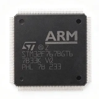
LPC4357JBD208K - ARM Cortex-M4/M0 MCU, 1MB Flash, 208-LQFP | NXP
MPN: LPC4357JBD208K ✓ 啟用中LPC4357JBD208K 概覽
An MCU (microcontroller unit) is a single-chip computer that integrates a CPU, memory (flash/SRAM), and programmable peripherals around a shared internal bus. The ARM Cortex-M family is a 32-bit RISC core family from Arm, and the Cortex-M4 (with FPU, DSP extensions) and Cortex-M0 (smallest, lowest-gate-count) are upward code- and tool-compatible, allowing a Cortex-M4 main core to be paired with a Cortex-M0 I/O coprocessor inside one chip. LPC43xx sits in NXP's high-performance MCU portfolio aimed at embedded applications that need both DSP-class signal processing and deterministic I/O.
Key features include dual-core asymmetric processing (M4 main + M0 coprocessor), 1 MB flash, 136 kB SRAM, 16 kB EEPROM, SPIFI for off-chip quad-SPI flash expansion, an SCT (State Configurable Timer) for complex PWM/capture sequences, SGPIO for high-speed serial I/O, two High-speed USB (one with on-chip HS PHY), Ethernet, an LCD controller supporting STN/TFT panels, and an EMC for SRAM/SDRAM/NOR/NAND. The 208-LQFP (28x28) package provides a thermal resistance suitable for industrial ambient operation with moderate copper pour.
Architecture depth: the Cortex-M4 core provides single-precision floating point and DSP (SIMD) instructions, while the Cortex-M0 coprocessor is intended to handle low-latency peripheral routines (for example, USB or motor-control loops) without disturbing the M4 application. A multi-layer AHB bus matrix routes independent masters (CPU, DMA, USB, Ethernet) to on-chip SRAM banks to minimize contention, and the SCT allows event-driven timing that can replace multiple capture/compare timers.
Typical applications include industrial drives and motor control (using SCT and dual cores), HMI panels (LCD + touch + Ethernet), USB peripherals and hubs (HS USB host/device), embedded connectivity gateways (Ethernet + SPIFI for large external flash), test and measurement instruments, and audio front ends that benefit from M4 DSP + M0 I/O separation.
When designing with this device, ensure the 208-LQFP power and ground pins are properly decoupled and that the SPIFI is only enabled when the application actually requires off-chip quad-SPI flash; otherwise keep it disabled to save power. Verify that the operating temperature grade (commercial 0 to 70 C, or industrial -40 to +85 C / -40 to +105 C depending on suffix) matches the end-equipment environment.
This page synthesizes distributor pricing, drop-in alternatives, and practical design notes not found in the manufacturer datasheet.
直接替換替代品,適用於 LPC4357JBD208K — 相同封裝,腳位對腳位相容。需重新設計 PCB 的不同封裝零件不列入。
此系列的變體
與下列產品可直接替換的同系列型號: LPC4357JBD208K (相同外形與佔位) — 差異在於 Package, Ethernet, SRAM, Core Architecture, Supply Voltage.
LPC4357JBD208
✅ 直接替換📋 參考替代品(不在目錄中)
LPC4357FET256
✅ 直接替換聯絡詢價
查看資料表 →LPC4330FET256
✅ 直接替換 ⚠️ 規格未經驗證聯絡詢價
查看資料表 →LPC4330FBD144
✅ 直接替換 ⚠️ 規格未經驗證聯絡詢價
查看資料表 →LPC4078FET208
✅ 直接替換 ⚠️ 規格未經驗證聯絡詢價
查看資料表 →LPC4357JBD208K 最大額定值與電氣特性
| Core Architecture | ARM Cortex-M4 (with FPU) + Cortex-M0 coprocessor |
| Bit Width | 32-bit |
| Number of Cores | 2 (dual-core asymmetric) |
| Maximum CPU Frequency | 204 MHz |
| Program Memory (Flash) | 1 MB (1M x 8) |
| SRAM | 136 kB |
| EEPROM | 16 kB |
| 供應電壓 | 3.3 V (typical) |
| 封裝 | 208-LQFP (28x28 mm) |
| 安裝類型 | Surface Mount |
| High-Speed USB | 2 ports (one with on-chip HS PHY) |
| Ethernet | 10/100 MAC included |
| Quad SPI Flash Interface (SPIFI) | Yes |
| External Memory Controller (EMC) | Yes (SRAM/SDRAM/NOR/NAND) |
| LCD Controller | Yes (STN/TFT) |
| State Configurable Timer (SCT) | Yes |
| Serial GPIO (SGPIO) | Yes |
| RoHS 狀態 | Compliant |
LPC4357JBD208K 208-lqfp (28x28 mm) 腳位配置指南
LPC4357JBD208K(208-lqfp (28x28 mm) 封裝)的腳位配置。 此數位 IC 包含 GPIO、通訊介面(UART、SPI、I2C)與電源腳位。替代腳位功能與配置選項請參閱製造商資料表。對嵌入式系統設計與 PCB 佈局至關重要。

無詳細腳位定義資料: LPC4357JBD208K.
請參閱 資料表 以查看完整腳位配置。
典型應用
LPC4357JBD208K 適用於 6 應用s: Industrial Motor Drives and Servo Control, Human-Machine Interface (HMI) Panels, USB Peripherals, Hubs, and Embedded Hosts, Industrial Ethernet Gateways and Protocol Bridges, Test and Measurement Instrumentation, Audio Front Ends and DSP Effects Processors.
Industrial Motor Drives and Servo Control
The LPC4357JBD208K fits industrial motor control because its Cortex-M4 core runs the FOC algorithm and current-sense DSP at up to 204 MHz while the Cortex-M0 coprocessor services time-critical SCT PWM updates without jitter. Per the NXP LPC43xx datasheet, the SCTimer/PWM supports complex PWM with dead-time insertion for 3-phase inverters, and the on-chip 16 kB EEPROM retains motor calibration parameters across power cycles. Typical designs pair the chip with NXP's MCUXpresso motor-control libraries and add external gate-driver IG (for example, an IRFS6307 or a gate driver pair) plus current-sense op-amps on the AVDD rail. Engineers achieve sub-microsecond control-loop determinism by dedicating the M0 to PWM via DMA, leaving the M4 application entirely free.
推薦
Human-Machine Interface (HMI) Panels
The LPC4357JBD208K is well matched to HMI panels because it integrates a TFT/STN LCD controller, 136 kB SRAM for frame buffering, Ethernet for network connectivity, and dual High-speed USB for touch-sensor and host-side maintenance. The Cortex-M4 + M0 split allows the M4 to handle graphics primitives and HMI logic while the M0 services the touch-sensor I2C interrupt and USB HID stack - no GUI blocking. Designers typically attach a 480x272 to 800x480 TFT LCD via the dedicated LCD interface, an RMII Ethernet PHY (LAN8720A-class) for Modbus-TCP/EtherCAT slave, and a capacitive touch controller on I2C. The SPIFI port enables affordable expansion of frame-buffer or asset graphics in off-chip quad-SPI flash without consuming internal 1 MB.
推薦
USB Peripherals, Hubs, and Embedded Hosts
The LPC4357JBD208K is purpose-built for USB peripherals because it integrates two High-speed USB controllers, one with an on-chip HS PHY, plus 1 MB flash and 136 kB SRAM that can host the full USB stack, vendor class drivers, and bulk endpoint buffers. The Cortex-M0 coprocessor offloads the USB interrupt service routine, while the M4 runs the application layer with no interrupt jitter. According to the LPC43xx datasheet, the USB controllers support host, device, and On-The-Go roles. Typical implementations include USB audio interfaces, USB mass-storage appliances, USB-to-UART bridges, and USB hubs with vendor control via GPIO. The chip's Ethernet MAC plus dual USB also enables USB-to-network bridging appliances at <300 mW active power.
推薦
Industrial Ethernet Gateways and Protocol Bridges
The LPC4357JBD208K serves industrial protocol gateways because its 10/100 Ethernet MAC plus dual High-speed USB plus 1 MB flash gives enough headroom for an embedded TCP/IP stack, Modbus-TCP server, EtherCAT slave, or PROFINET IO device alongside the fieldbus translator. The Cortex-M4 handles the gateway application while the Cortex-M0 services the Ethernet DMA descriptors and the USB device stack in parallel. EMC (External Memory Controller) allows attaching a fast SRAM or SDRAM for large packet buffers when bridging 1+ Gbps aggregate traffic. Engineers typically pair the chip with an external RMII PHY and a watchdog supervisor (TPS3823-class) for IEC 61131-2 compliance.
推薦
Test and Measurement Instrumentation
The LPC4357JBD208K fits T&M instruments because the Cortex-M4 DSP extensions process FFTs, FIR filters, and PID loops in real time, while the Cortex-M0 services the high-speed ADC via DMA or SGPIO without disturbing the main thread. Per the LPC43xx datasheet, the chip's 204 MHz headroom supports up to ~100 kHz sample rates on a 4-channel SAR ADC for power-quality analyzers, oscilloscope front ends, or multi-meter platforms. The LCD controller drives 320x240 mono/color panels typically used in handheld T&M. SPIFI lets designers add large asset libraries or calibration tables in off-chip flash without sacrificing the 1 MB internal flash budget for code.
推薦
Audio Front Ends and DSP Effects Processors
The LPC4357JBD208K suits audio front ends because the Cortex-M4 FPU + DSP extensions run biquad filters, reverb, and dynamics processing at up to 204 MHz while the Cortex-M0 handles USB Audio Class 1.0/2.0 streaming and I2S DMA without glitching. The chip's dual High-speed USB controllers support USB Audio at 24-bit/96 kHz, while the I2S ports connect to external DACs (for example, PCM1794A-class) and ADCs. The 136 kB SRAM is enough for typical audio effect delays and convolution buffers. Designers can also use the LCD controller to drive a small graphic display for level meters, and the SCTimer for precise sample-rate-clock generation tied to USB SOF packets.
推薦
推薦產品摘要
工程參考資料,適用於 LPC4357JBD208K — 比較、設計指引及合規資訊。
選型指南
與替代品比較
| 參數 | 本產品 | LPC4357JBD208 | LPC4357FET256 | LPC4330FET256 | LPC4330FBD144 | LPC4078FET208 |
|---|---|---|---|---|---|---|
| Brand | NXP Semiconductors | NXP Semiconductors | NXP Semiconductors | NXP Semiconductors | NXP Semiconductors | NXP Semiconductors |
| Package | 208-LQFP (28x28) | 208-LQFP (28x28) - same | 256-LBGA (17x17) - different | 256-LBGA (17x17) - different | 144-LQFP (20x20) - different | 208-LQFP - same family |
| Core Architecture | Cortex-M4 + Cortex-M0 dual-core | Cortex-M4 + Cortex-M0 dual-core | Cortex-M4 + Cortex-M0 dual-core | Cortex-M4 + Cortex-M0 dual-core | Cortex-M4 + Cortex-M0 dual-core | Cortex-M4 single-core (no M0) |
| Maximum CPU Frequency | 204 MHz | 204 MHz | 204 MHz | 204 MHz | 204 MHz | 120 MHz |
| High-Speed USB | 2 ports (one with on-chip HS PHY) | 2 ports (one with on-chip HS PHY) | 2 ports (one with on-chip HS PHY) | 2 ports (one with on-chip HS PHY) | 2 ports (one with on-chip HS PHY) | 1 port (no HS PHY) |
| Ethernet MAC | 10/100 (PHY external) | 10/100 (PHY external) | 10/100 (PHY external) | 10/100 (PHY external) | 10/100 (PHY external) | 10/100 (PHY external) |
| Pin-to-Pin Compatible with LPC4357JBD208K | Yes (this product) | Yes | No (BGA-256) | No (BGA-256) | No (LQFP-144) | No (single-core) |
主要差異化特點
- Dual-core Cortex-M4 + Cortex-M0 asymmetric multiprocessing in a 208-LQFP (對比LPC4078FET208)
- Latest silicon revision 'K' suffix vs legacy 'E' revision (對比LPC4357JBD208E)
- More on-chip SRAM (136 kB) than legacy LPC18xx (對比LPC1833JBD144)
- Quad-SPI Flash Interface (SPIFI) integrated (對比LPC4078FET208)
設計說明
The 208-LQFP package requires a 28x28 mm land pattern with 0.5 mm pitch pads. Route power (VDD, VDDIO) and ground (VSS) as wide polygons to all pins, and place at least one 100 nF X7R decoupling capacitor per pair of VDD/VSS pins as close as physically possible to the package - the LPC4357 has 15+ power/ground pairs across the package. Add bulk 4.7 uF ceramic + 10 uF electrolytic capacitors near the regulator input pins. Per NXP design guidelines, keep all high-speed traces (Ethernet RMII, USB DP/DM, SPIFI CLK) length-matched and ground-referenced.
The LPC4357JBD208K requires 3.3 V for the main VDD and a separate 3.3 V analog supply for AVDD/VDDA if used. The internal core runs at 1.2 V generated by the on-chip voltage regulator - decouple VCORE pins with 1 uF X7R per the datasheet. Estimated: at 204 MHz full activity, core current is approximately 100 mA, USB HS PHY adds ~30 mA, and Ethernet MAC adds ~25 mA, so the 3.3 V regulator must supply at least 250 mA with 20% headroom (300 mA minimum). A low-noise LDO such as LP5900TLX-1.8 (or 3.3 V equivalent) is recommended for analog rails. Power-up sequencing: hold RESET until 3.3 V is stable, then release after the 32 kHz crystal stabilizes.
Do not enable SPIFI unless your design actually requires off-chip quad-SPI flash; leaving it enabled without a populated flash chip can cause boot failure on parts that look for SPIFI image at boot. Also, the 'K' suffix indicates industrial-grade temperature but always cross-check the exact TA range in the LPC43xx datasheet's electrical characteristics before final qualification. Verify the EMC pin mapping matches your SDRAM data-width configuration (8/16/32-bit) and that the EMC clock divider is consistent with the SDRAM tCK requirement.
Route USB DP/DM as a 90-ohm differential pair with ground reference and length matching within 150 mil. For Ethernet RMII, route the 50 MHz reference clock with controlled impedance and keep the PHY-to-MCU traces short (<50 mm). Place the 32.768 kHz crystal within 5 mm of the XTAL1/XTAL2 pins and ground its load capacitors to a quiet ground island. Avoid routing SPIFI CLK near the LCD data bus to minimize crosstalk. Always provide a robust reset circuit (RC or supervisor such as TPS3823) - relying on internal POR alone can cause brown-out issues under heavy loads.
合規資訊
RoHS and lead-free per DigiKey listing and NXP product page. AEC-Q100 not applicable (general-purpose MCU, not automotive qualified unless 'K' suffix designates AEC-Q100 - confirm with datasheet). Halogen-free status not explicitly stated in web data.