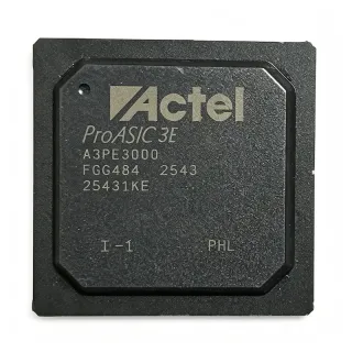
M2GL060-FGG484I - 56.5K LEs, 267 I/O IGLOO2 FPGA | Microchip
MPN: M2GL060-FGG484I ✓ 啟用中M2GL060-FGG484I 概覽
An FPGA is a programmable semiconductor containing configurable logic blocks, programmable interconnect, and input/output resources. It belongs to the programmable-logic hierarchy, alongside CPLDs, and provides higher logic density and more flexible routing than basic combinational devices. The IGLOO2 family is positioned for compact, low-power embedded systems that require deterministic hardware functions without the cost or complexity of an application processor.
The M2GL060 provides 56.5K logic elements, 267 I/Os, and approximately 1826 kb of RAM according to the product listing data. Because the device uses embedded flash configuration, the bitstream is retained in nonvolatile memory, allowing the FPGA to operate without a separate external configuration PROM. A 484-ball BGA also provides more board interconnect than the smaller IGLOO2 packages and supports designs with extensive parallel or high-speed interfaces.
IGLOO2 devices support communications, industrial, medical, defense, and aviation applications. Microchip describes the family for Gigabit Ethernet and dual PCI Express control planes, bridging, I/O expansion and conversion, video and image processing, system management, and secure connectivity. The combination of configurable logic and 267 I/Os allows designers to consolidate protocol converters, interface controllers, and supervisory logic into one device.
The M2GL060-FGG484I is appropriate when a design needs more I/O than a small CPLD but does not require a higher-density FPGA or an embedded hard processor. It can also serve as a companion logic device beside a microprocessor in industrial controllers, medical instruments, communication modules, and embedded imaging systems. Its 484-FBGA footprint demands careful escape-routing, via-in-pad awareness, and assembly-process planning.
For PCB implementation, follow the Microchip IGLOO2 packaging and pin-description user guide for bank assignments, package dimensions, and pin compatibility. Confirm the selected PCB footprint and assembly process against the package drawings before layout release, and use the device-specific programming and configuration workflow when creating the bitstream.
This page consolidates device capacity, package, interface, and lifecycle information with drop-in same-footprint alternatives, application guidance, and practical design notes. It supports faster component selection while keeping board-level decisions tied to Microchip's package and user-guide documentation.
直接替換替代品,適用於 M2GL060-FGG484I — 相同封裝,腳位對腳位相容。需重新設計 PCB 的不同封裝零件不列入。
此系列的變體
與下列產品可直接替換的同系列型號: M2GL060-FGG484I (相同外形與佔位) — 差異在於 Configuration Memory, Logic Elements, Device Type, Maximum Operating Temperature, Minimum Operating Temperature.
M2GL060-FG484I
✅ 直接替換聯絡詢價
查看資料表 →M2GL060-FGG484
✅ 直接替換聯絡詢價
查看資料表 →M2GL060T-FGG484I
✅ 直接替換📋 參考替代品(不在目錄中)
M2GL060T-1FGG484I
✅ 直接替換📋 參考替代品(不在目錄中)
M2GL060-1FG484I
✅ 直接替換📋 參考替代品(不在目錄中)
M2GL060-FGG484I 最大額定值與電氣特性
| Device Type | Low-density flash FPGA |
| FPGA Family | IGLOO2 |
| Logic Elements | 56.5K LEs |
| User I/O Count | 267 I/O |
| Embedded RAM | 1826 kb |
| Configuration Memory | Embedded flash |
| 封裝 | 484-FBGA |
| Package Type | Fine-pitch BGA |
| Number of Balls | 484 balls |
| Product Status | In Production |
| 安裝類型 | Surface mount |
| Manufacturer | Microchip Technology |
M2GL060-FGG484I fine-pitch bga 腳位配置指南
M2GL060-FGG484I(fine-pitch bga 封裝)的腳位配置。 此數位 IC 包含 GPIO、通訊介面(UART、SPI、I2C)與電源腳位。替代腳位功能與配置選項請參閱製造商資料表。對嵌入式系統設計與 PCB 佈局至關重要。

無詳細腳位定義資料: M2GL060-FGG484I.
請參閱 資料表 以查看完整腳位配置。
典型應用
M2GL060-FGG484I 適用於 6 應用s: Industrial Control and System Management, Communications Protocol Bridging, Medical Instrumentation and Data Acquisition, Video and Image Processing Support, Embedded Imaging and Camera Interface, Secure Connectivity and Device Control.
Industrial Control and System Management
The M2GL060-FGG484I suits industrial controllers that need programmable supervisory logic, machine-state sequencing, and multiple peripheral interfaces. Its 56.5K logic elements can consolidate condition monitoring, timing, and interlock functions that would otherwise occupy several small programmable devices, while 267 I/Os provide flexible connections to sensors, actuators, and human-interface boards. The 484-FBGA package also supports designs requiring a high contact count. Implementation should account for industrial temperature requirements, isolated interfaces, and deterministic timing before releasing the configuration.
推薦
Communications Protocol Bridging
The M2GL060-FGG484I is well suited to protocol-bridge and control-plane logic in communication equipment. With 56.5K logic elements and 267 I/Os, it can translate interfaces, supervise link state, and implement buffering or framing functions beside a host processor. Microchip specifically identifies bridging, Gigabit Ethernet, and dual PCI Express control-plane uses for the IGLOO2 family. The large BGA package gives designers access to many I/Os for parallel data paths, but high-speed layout must follow the manufacturer's bank and pin-assignment guidance.
推薦
Medical Instrumentation and Data Acquisition
The M2GL060-FGG484I can serve as a configurable data-acquisition and supervisory engine in medical instruments. Its programmable fabric supports sensor multiplexing, control sequencing, and digital filtering, while 267 I/Os allow connection to analog front ends and precision converters. Medical designs require careful isolation, creepage, leakage, and electromagnetic-compatibility planning in addition to device qualification. Verify the exact ordering code's temperature and qualification attributes against the instrument's environmental requirements before using it in a safety-related signal path.
推薦
Video and Image Processing Support
The M2GL060-FGG484I fits parallel image-processing support, sensor-format conversion, and timing-generation functions where deterministic programmable logic is required. The 267 available I/Os are valuable for connecting pixel buses, synchronization signals, and control lines, while embedded flash permits a self-contained configuration. IGLOO2 is identified by Microchip as suitable for video and image-processing applications. Actual throughput depends on the chosen I/O standards, clocking, and timing closure, so prototype the critical interface and use the device timing tools before committing to a high-volume layout.
推薦
Embedded Imaging and Camera Interface
The M2GL060-FGG484I can implement camera capture timing, sensor control, and data-path adaptation in embedded imaging equipment. Its 56.5K logic elements provide capacity for parallel-to-serial conversion, pixel-clock generation, and pipeline control without requiring a high-end processor, while 267 I/Os support extensive sensor and memory connectivity. Designers should use the Microchip pin and bank guidance to place interfaces in electrically compatible groups and preserve timing margin on high-speed links. Power sequencing and I/O voltage selection are equally important in compact camera modules.
推薦
Secure Connectivity and Device Control
The M2GL060-FGG484I fits secure-connectivity appliances, peripheral controllers, and interface-conversion modules where a flexible amount of programmable logic is preferable to a fixed-function device. Microchip lists secure connectivity and system management as intended IGLOO2 uses. The embedded flash configuration supports a repeatable field-update workflow, and 267 I/Os allow multiple external devices to be connected without a second programmable-logic package. Validate encryption-related implementation requirements, security lifecycle expectations, and any sector-protection needs against the specific programming flow before production deployment.
推薦
推薦產品摘要
工程參考資料,適用於 M2GL060-FGG484I — 比較、設計指引及合規資訊。
選型指南
Select M2GL060-FG484I or M2GL060-FGG484 when their documented ordering attributes satisfy the design and the required grade code matches. Consider M2GL060T-FGG484I or M2GL060T-1FGG484I when the manufacturer's ordering information confirms the appropriate T configuration or speed designation. Use M2GL060-1FG484I only after confirming its speed, temperature, and qualification requirements. A different manufacturer's FPGA should not be treated as a drop-in option because device resources, voltage, pinout, and programming tools differ. Final selection requires comparison against the complete M2GL060 datasheet and the intended assembly process.
與替代品比較
| 參數 | 本產品 | M2GL060-FG484I | M2GL060-FGG484 | M2GL060T-FGG484I | M2GL060T-1FGG484I | M2GL060-1FG484I |
|---|---|---|---|---|---|---|
| Brand | Microchip Technology | Microchip Technology | Microchip Technology | Microchip Technology | Microchip Technology | Microchip Technology |
| Package | 484-FBGA | 484-FBGA | 484-FBGA | 484-FBGA | 484-FBGA | 484-FBGA |
| FPGA Family | IGLOO2 | IGLOO2 | IGLOO2 | IGLOO2 | IGLOO2 | IGLOO2 |
| Logic Elements | 56.5K LEs | 56.5K LEs | 56.5K LEs | 56.5K LEs | 56.5K LEs | 56.5K LEs |
| User I/O | 267 I/O | 267 I/O | 267 I/O | 267 I/O | 267 I/O | 267 I/O |
| Embedded RAM | 1826 kb | 1826 kb | 1826 kb | 1826 kb | 1826 kb | 1826 kb |
| Configuration Memory | Embedded flash | Embedded flash | Embedded flash | Embedded flash | Embedded flash | Embedded flash |
| Ordering Code Difference | FGG484I | FG484I | FGG484 | T-FGG484I | T-1FGG484I | 1FG484I |
主要差異化特點
- Matches the same 484-FBGA M2GL060 family with 56.5K logic elements and 267 I/Os (對比M2GL060-FG484I)
- Supports a broad range of general-purpose programmable functions in one package (對比M2GL060T-FGG484I)
- Provides 267 user I/Os for interface-heavy industrial and communications designs (對比M2GL060-FGG484)
設計說明
The M2GL060-FGG484I uses a 484-FBGA footprint, so the PCB design must follow the manufacturer package drawing and recommended land pattern rather than a generic BGA rule. Preserve the documented ball assignments and bank structure when placing memory, clocks, and high-speed interfaces. Confirm that the assembly process supports the required ball pitch, pad geometry, and thermal-relief strategy before releasing the fabrication package.
Assign related high-speed signals to the same compatible I/O bank and route clocks, configuration access, and critical data paths with controlled length matching. Use the IGLOO 2 FPGA Packaging and Pin Descriptions User Guide to identify bank assignments and permitted voltage combinations. Avoid long stubs between the BGA and external components because they can create reflection and timing-margin problems on fast interfaces.
Create separate, well-decoupled supply paths for the core and each I/O bank, then validate every bank voltage against the selected device speed grade and interface standard. Place bulk and high-frequency decoupling close to the associated supply and ground balls. Because power depends on configured logic, clock activity, and I/O toggling, estimate the finished design with the device power tools and verify it on hardware under worst-case activity.
Do not assume that every M2GL060 suffix is interchangeable. The FGG484I, FG484I, T-FGG484I, T-1FGG484I, and 1FG484I orderings share the 484-FBGA family, but speed, temperature, qualification, and commercial-code requirements can differ. Run the exact candidate through Microchip's cross-reference and ordering tools, and confirm the programmed bitstream is compatible before treating a substitution as a drop-in change.
合規資訊
The device is listed as in production by Microchip. Exact RoHS, REACH, halogen-free, conflict-minerals, and qualification statements for this ordering code require confirmation from the manufacturer product documentation or a current compliance declaration.