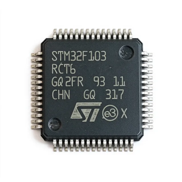
STM32F103RCT6 - 72MHz Cortex-M3 MCU, 256KB Flash | ST
MPN: STM32F103RCT6 ✓ 啟用中| 數量 | 單價 | 小計 |
|---|---|---|
| 1 | $2.8125 | $2.81 |
| 10 | $2.0313 | $20.31 |
| 100 | $1.7969 | $179.69 |
| 500 | $1.7188 | $859.40 |
| 1,000 | $1.6406 | $1,640.60 |
STM32F103RCT6 概覽
A microcontroller (MCU) is a compact integrated circuit that combines a processor core, memory, and programmable peripherals on a single chip, forming the central control element of embedded systems. The STM32F103RCT6 sits within the STM32 family hierarchy: STM32F1 series -> STM32 MCU portfolio -> ARM Cortex-M based microcontrollers -> semiconductor ICs. The Cortex-M3 core, with its nested vectored interrupt controller (NVIC) and memory protection unit (MPU), delivers deterministic real-time performance at 1.25 DMIPS/MHz.
Key features include a wide 2.0V to 3.6V supply range, -40C to +85C industrial temperature operation, Sleep/Stop/Standby low-power modes, a real-time clock (RTC), multiple PWM-capable timers, and 5V-tolerant GPIOs. The 256KB high-density Flash accommodates complex firmware such as RTOS-based applications, while rich peripheral integration reduces external BOM cost and board area.
Architecturally, the device uses an AMBA AHB/APB bus matrix connecting the 72MHz core to SRAM and peripherals, with single-cycle hardware multiply for efficient control-loop mathematics. Three 12-bit ADCs run at up to 1 MSPS (2 MSPS in interleaved dual mode), and two 12-bit DACs support analog output. Connectivity includes USB 2.0 Full Speed, CAN 2.0B, three USARTs, SPI, and I2C interfaces.
Typical applications include industrial motor control, PLCs, medical devices, IoT gateways, USB/CAN communication bridges, and HMI panels.
Design tip: decouple every VDD pin with 100nF close to the pin plus a 4.7uF bulk capacitor, filter VDDA through a ferrite bead, and strap BOOT0 correctly for the intended boot mode.
This page synthesizes distributor pricing, drop-in alternatives including the GigaDevice GD32F103RCT6, pinout guidance, and practical design notes not found in the manufacturer datasheet.
直接替換替代品,適用於 STM32F103RCT6 — 相同封裝,腳位對腳位相容。需重新設計 PCB 的不同封裝零件不列入。
此系列的變體
與下列產品可直接替換的同系列型號: STM32F103RCT6 (相同外形與佔位) — 差異在於 Package, Timers, Operating Temperature, ADC, Communication Interfaces.
快速比較工具 — 選擇替代零件進行並排比較:
STM32F103RET6
✓ 有庫存
$2.2148 / 單位
查看資料表 →STM32F103RBT6
聯絡詢價
查看資料表 →STM32F107RCT6
聯絡詢價
查看資料表 →STM32F303RCT6
聯絡詢價
查看資料表 →GD32F103RCT6
📋 參考替代品(不在目錄中)
STM32F103RCT6 最大額定值與電氣特性
| Core | ARM Cortex-M3 32-bit |
| 最大時脈頻率 | 72 MHz |
| Flash Memory | 256 KB |
| SRAM | 48 KB |
| Supply Voltage Range | 2.0 V to 3.6 V |
| 工作溫度 | -40C to +85C |
| 封裝 | LQFP64 (10x10 mm) |
| GPIO Count | 51 |
| ADC | 3 x 12-bit, up to 1 MSPS (2 MSPS interleaved) |
| DAC | 2 x 12-bit |
| USB | USB 2.0 Full Speed |
| CAN | 2 x CAN 2.0B |
| USART | 3 x USART/UART |
| Timers | Multiple 16-bit timers including PWM, plus RTC |
| Processing Performance | 1.25 DMIPS/MHz |
| Low-Power Modes | Sleep, Stop, Standby |
| 安裝類型 | Surface Mount |
| RoHS 狀態 | Compliant |
STM32F103RCT6 lqfp64 (10x10 mm) 腳位配置指南
STM32F103RCT6(lqfp64 (10x10 mm) 封裝)的腳位配置。 此數位 IC 包含 GPIO、通訊介面(UART、SPI、I2C)與電源腳位。替代腳位功能與配置選項請參閱製造商資料表。對嵌入式系統設計與 PCB 佈局至關重要。

無詳細腳位定義資料: STM32F103RCT6.
請參閱 資料表 以查看完整腳位配置。
典型應用
STM32F103RCT6 適用於 6 應用s: Industrial Motor Control, USB and CAN Communication Bridges, IoT Gateways and Sensor Nodes, Medical and Diagnostic Devices, HMI Panels and Display Controllers, PLC and Industrial Automation Logic.
Industrial Motor Control
The STM32F103RCT6 fits motor-control drives through its three 12-bit ADCs running at up to 1 MSPS (2 MSPS interleaved), which capture dual-shunt phase currents with enough resolution for field-oriented control (FOC). Advanced PWM-capable timers generate complementary outputs with dead-time insertion for three-phase inverters, while the 72MHz Cortex-M3 core executes control loops at 1.25 DMIPS/MHz with deterministic NVIC interrupt latency. The -40C to +85C rating suits drive enclosures. Unlike 8-bit MCUs, this device closes current loops in tens of microseconds while leaving headroom for communication protocols on the dual CAN 2.0B buses used in factory networks.
推薦
USB and CAN Communication Bridges
With native USB 2.0 Full Speed device and two CAN 2.0B controllers on one chip, the STM32F103RCT6 is a natural fit for USB-to-CAN gateways used in vehicle diagnostics and industrial fieldbus tooling. The USB peripheral takes its 48MHz reference from the PLL, enabling crystal-accurate USB timing, while the bxCAN controllers handle 1 Mbit/s arbitration and hardware filtering without CPU load. The 256KB Flash holds USB class stacks plus protocol converters simultaneously. Compared with a discrete USB-to-CAN chip pair, this single-chip approach cuts BOM cost and board area while the 48KB SRAM buffers burst traffic.
推薦
IoT Gateways and Sensor Nodes
The STM32F103RCT6 serves IoT gateway nodes where multiple sensor interfaces converge: three USARTs, SPI, I2C, and 51 GPIOs connect radios, meters, and actuators, while Sleep/Stop/Standby modes reduce average current in battery-backed installations. The 256KB Flash accommodates an RTOS plus TLS-secured firmware images, and the RTC maintains timestamps through low-power states. Standby mode drops consumption to microamp levels per the ST datasheet, enabling years of operation from primary cells in duty-cycled designs. Compared with smaller F1 parts, the RCT6's 48KB SRAM comfortably hosts network protocol stacks with packet buffers for mesh or cellular modems.
推薦
Medical and Diagnostic Devices
Portable medical instruments benefit from the STM32F103RCT6's combination of three 12-bit ADCs for biopotential or pressure-sensor acquisition, 12-bit DACs for stimulus generation, and USB Full Speed for data offload to host PCs. The 2.0V to 3.6V single-supply operation simplifies battery-powered power trees, and filtering VDDA preserves ADC effective resolution for microvolt-level signals. The 256KB Flash holds calibration tables, digital filtering, and USB device firmware together. Designers should follow ST's EMC layout guidance and add isolation on patient-connected interfaces; the deterministic Cortex-M3 interrupt architecture supports fixed-rate sampling loops needed for reliable waveform capture.
推薦
HMI Panels and Display Controllers
For membrane-key and small-TFT human-machine interfaces, the STM32F103RCT6 drives displays over SPI or parallel FSMC buses while scanning touch inputs on its 5V-tolerant GPIOs. The 256KB Flash stores fonts, bitmap assets, and GUI frameworks that exceed smaller F1 parts, and 48KB SRAM supports framebuffer sections and message queues for touch events. USART and CAN links connect the panel to PLCs or motor drives, making it a compact operator terminal for industrial equipment. Typical implementations pair the MCU with ST's legacy touch-sensing libraries; the -40C to +85C range and RoHS compliance suit panel installation in factory environments without active cooling.
推薦
PLC and Industrial Automation Logic
The STM32F103RCT6 implements compact PLC logic modules where dual CAN 2.0B buses, three USARTs, and abundant timers replace discrete ladder-logic hardware. Hardware PWM outputs drive actuators and dimmers, input-capture timers measure pulse frequencies from encoders and flow meters, and the RTC schedules event logs - all on a chip operating reliably from -40C to +85C on a single 3.3V rail. The 256KB Flash supports modular firmware with OTA-update bootloaders, a growing requirement in industrial retrofit markets. Compared with legacy 8-bit PLC cores, the 72MHz Cortex-M3 executes PID loops and protocol stacks concurrently within deterministic NVIC-driven scheduling.
推薦
推薦產品摘要
工程參考資料,適用於 STM32F103RCT6 — 比較、設計指引及合規資訊。
選型指南
與替代品比較
| 參數 | 本產品 | STM32F103RET6 | STM32F103RBT6 | STM32F107RCT6 | GD32F103RCT6 |
|---|---|---|---|---|---|
| Package | LQFP64 (10x10 mm) | LQFP64 - same | LQFP64 - same | LQFP64 - same | LQFP64 - same |
| Brand | STMicroelectronics | STMicroelectronics | STMicroelectronics | STMicroelectronics | GigaDevice |
| Core / Max Clock | Cortex-M3 / 72 MHz | Cortex-M3 / 72 MHz | Cortex-M3 / 72 MHz | Cortex-M3 / 72 MHz | Cortex-M3 / 108 MHz |
| Flash Memory | 256 KB | 512 KB | 128 KB | 256 KB | 256 KB |
| SRAM | 48 KB | 64 KB | 20 KB | 64 KB | 48 KB |
| ADC | 3 x 12-bit, 1 MSPS | 3 x 12-bit, 1 MSPS | 3 x 12-bit, 1 MSPS | 2 x 12-bit, 1 MSPS | 3 x 12-bit, ~1 MSPS |
| USB / CAN | USB FS / 2 x CAN 2.0B | USB FS / 2 x CAN | USB FS / 1 x CAN | USB OTG FS / 2 x CAN / Ethernet MAC | USB FS / 2 x CAN |
| GPIO Count | 51 | 51 | 51 | 51 | 51 |
| Drop-in Compatibility Notes | Reference part | Pin-to-pin, larger memory, higher cost | Pin-to-pin, smaller memory, lower cost | Pin-to-pin, connectivity line, firmware review needed | P2P candidate, board revalidation required |
主要差異化特點
- Balanced memory for mid-size firmware (對比STM32F103RBT6)
- Dual CAN 2.0B controllers (對比STM32F103RBT6)
- Proven ST ecosystem vs Chinese clone (對比GD32F103RCT6)
- Cost-efficient entry vs larger RET6 (對比STM32F103RET6)
設計說明
Decouple every VDD/VSS pair with a 100nF ceramic capacitor placed within 2-3 mm of the pin, plus a single 4.7uF bulk capacitor near the LQFP64. Route a separate filtered supply to VDDA through a ferrite bead (e.g., 600 ohm at 100 MHz) with its own 100nF + 1uF pair - VDDA noise directly shifts ADC codes. Expose the USB D+/D- pair as a 90-ohm differential route with series 22-ohm resistors at the pins, and keep the 1.5k pull-up on D+ for full-speed enumeration per the ST USB design references.
BOOT0 must not float: strap it to ground with a 10k resistor for flash boot, and expose a jumper to 3.3V for system-memory (UART) bootloader access. PB2 (BOOT1) also affects boot configuration. During debugging note that PA13/PA14 are shared with SWDIO/SWCLK - never repurpose them in hardware that must remain debuggable. When migrating to GD32F103RCT6, recheck flash wait states and USB timing because the zero-wait-state flash behavior differs from ST silicon.
Estimated: with all peripherals clocked at 72 MHz, the STM32F103RCT6 consumes on the order of 36-50 mA (per ST datasheet typical figures for the high-density line), so a 100 mA-class 3.3V regulator such as an LDO with 150 mA capability is sufficient headroom for the MCU plus a small transceiver. Standby mode reduces consumption to a few microamps, enabling RTC-backed battery designs. In Stop mode, wake latency is under a few microseconds via EXTI lines, suitable for duty-cycled battery nodes - size the regulator for the active current, not standby.
For the 8 MHz HSE crystal, keep traces under 10 mm with ground guarding, and load capacitors per the crystal datasheet (typically 12-22 pF) - USB and CAN timing depend on HSE accuracy, so use a crystal with +/-30 ppm or better tolerance. Route CAN_TX/RX away from switching-regulator nodes and terminate the CAN bus with 120 ohm at both ends. On ADC inputs, add an RC anti-alias filter (e.g., 1k + 10 nF) since the SAR ADC injects charge kickback during sampling.
合規資訊
RoHS compliant and lead-free per STMicroelectronics product data for STM32F103RCT6. REACH, halogen-free, and conflict-minerals status not stated in provided data.

